-
 Agriculture
-
 Health-Care
-
 Environment
-
 Construction-Real-Estate
-
 Tools-Hardware
-
 Home-Garden
-
 Furniture
-
 Luggage-Bags-Cases
-
 Medical-devices-Supplies
-
 Gifts-Crafts
-
 Sports-Entertainment
-
 Food-Beverage
-
 Vehicles-Transportation
-
 Power-Transmission
-
 Material-Handling
-
 Renewable-Energy
-
 Safety
-
 Testing-Instrument-Equipment
-
 Construction-Building-Machinery
-
 Pet-Supplies
-
 Personal-Care-Household-Cleaning
-
 Vehicle-Accessories-Electronics-Tools
-
 School-Office-Supplies
-
 Packaging-Printing
-
 Mother-Kids-Toys
-
 Business-Services
-
 Commercial-Equipment-Machinery
-
 Apparel-Accessories
-
 Security
-
 Shoes-Accessories
-
 Vehicle-Parts-Accessories
-
 Jewelry-Eyewear-Watches-Accessories
-
 Lights-Lighting
-
 Fabric-Textile-Raw-Material
-
 Fabrication-Services
-
 Industrial-Machinery
-
 Consumer-Electronics
-
 Electrical-Equipment-Supplies
-
 Electronic-Components-Accessories-Telecommunications
-
 Home-Appliances
-
 Beauty
-
 Chemicals
-
 Rubber-Plastics
-
 Metals-Alloys
- Masonry Materials
- Curtain Walls & Accessories
- Earthwork Products
- Fireproofing Materials
- Heat Insulation Materials
- Plastic Building Materials
- Building Boards
- Soundproofing Materials
- Timber
- Waterproofing Materials
- Balustrades & Handrails
- Bathroom & Kitchen
- Flooring & Accessories
- Tiles & Accessories
- Door, Window & Accessories
- Fireplaces & Stoves
- Floor Heating Systems & Parts
- Stairs & Stair Parts
- Ceilings
- Elevators & Escalators
- Stone
- Countertops, Vanity Tops & Table Tops
- Mosaics
- Metal Building Materials
- Multifunctional Materials
- Ladders & Scaffoldings
- Mouldings
- Corner Guards
- Decorative Films
- Formwork
- Building & Industrial Glass
- Other Construction & Real Estate
- Wallpapers/Wall panels
- HVAC System & Parts
- Outdoor Facilities
- Prefabricated Buildings
- Festive & Party Supplies
- Bathroom Products
- Household Sundries
- Rain Gear
- Garden Supplies
- Household Cleaning Tools & Accessories
- Lighters & Smoking Accessories
- Home Storage & Organization
- Household Scales
- Smart Home Improvement
- Home Textiles
- Kitchenware
- Drinkware & Accessories
- Dinnerware, Coffee & Wine
- Home Decor
- Golf
- Fitness & Body Building
- Amusement Park Facilities
- Billiards, Board Game,Coin Operated Games
- Musical Instruments
- Outdoor Affordable Luxury Sports
- Camping & Hiking
- Fishing
- Sports Safety&Rehabilitation
- Ball Sports Equipments
- Water Sports
- Winter Sports
- Luxury Travel Equipments
- Sports Shoes, Bags & Accessories
- Cycling
- Other Sports & Entertainment Products
- Artificial Grass&Sports Flooring&Sports Court Equipment
- Scooters
- Food Ingredients
- Honey & Honey Products
- Snacks
- Nuts & Kernels
- Seafood
- Plant & Animal Oil
- Beverages
- Fruit & Vegetable Products
- Frog & Escargot
- Bean Products
- Egg Products
- Dairy Products
- Seasonings & Condiments
- Canned Food
- Instant Food
- Baked Goods
- Other Food & Beverage
- Meat & Poultry
- Confectionery
- Grain Products
- Feminie Care
- Hair Care & Styling
- Body Care
- Hands & Feet Care
- Hygiene Products
- Men's Grooming
- Laundry Cleaning Supplies
- Travel Size & Gift Sets
- Room Deodorizers
- Other Personal Care Products
- Pest Control Products
- Special Household Cleaning
- Floor Cleaning
- Kitchen & Bathroom Cleaning
- Oral Care
- Bath Supplies
- Yellow Pages
- Correction Supplies
- Office Binding Supplies
- Office Cutting Supplies
- Board Erasers
- Office Adhesives & Tapes
- Education Supplies
- Pencil Cases & Bags
- Notebooks & Writing Pads
- File Folder Accessories
- Calendars
- Writing Accessories
- Commercial Office Supplies
- Pencil Sharpeners
- Pens
- Letter Pad/Paper
- Paper Envelopes
- Desk Organizers
- Pencils
- Markers & Highlighters
- Filing Products
- Art Supplies
- Easels
- Badge Holder & Accessories
- Office Paper
- Printer Supplies
- Book Covers
- Other Office & School Supplies
- Stationery Set
- Boards
- Clipboards
- Stamps
- Drafting Supplies
- Stencils
- Electronic Dictionary
- Books
- Map
- Magazines
- Calculators
- Baby & Toddler Toys
- Educational Toys
- Classic Toys
- Dress Up & Pretend Play
- Toy Vehicle
- Stuffed Animals & Plush Toys
- Outdoor Toys & Structures
- Balloons & Accessories
- Baby Food
- Children's Clothing
- Baby Supplies & Products
- Maternity Clothes
- Kids Shoes
- Baby Care
- Novelty & Gag Toys
- Dolls & Accessories
- Puzzle & Games
- Blocks & Model Building Toys
- Toddler Clothing
- Baby Clothing
- Kids' Luggage & Bags
- Arts, Crafts & DIY Toys
- Action & Toy Figures
- Baby Appliances
- Hobbies & Models
- Remote Control Toys
- Promotional Toys
- Pregnancy & Maternity
- Hygiene Products
- Kid's Textile&Bedding
- Novelty & Special Use
- Toy Weapons
- Baby Gifts
- Baby Storage & Organization
- Auto Drive Systems
- ATV/UTV Parts & Accessories
- Marine Parts & Accessories
- Other Auto Parts
- Trailer Parts & Accessories
- Auto Transmission Systems
- Train Parts & Accessories
- Universal Parts
- Railway Parts & Accessories
- Auto Brake Systems
- Aviation Parts & Accessories
- Truck Parts & Accessories
- Auto Suspension Systems
- Auto Lighting Systems
- New Energy Vehicle Parts & Accessories
- Auto Steering Systems
- Wheels, Tires & Accessories
- Bus Parts & Accessories
- Auto Performance Parts
- Cooling System
- Go-Kart & Kart Racer Parts & Accessories
- Air Conditioning Systems
- Heavy Duty Vehicle Parts & Accessories
- Auto Electrical Systems
- Auto Body Systems
- Auto Engine Systems
- Container Parts & Accessories
- Motorcycle Parts & Accessories
- Refrigeration & Heat Exchange Equipment
- Machine Tool Equipment
- Food & Beverage Machinery
- Agricultural Machinery & Equipment
- Apparel & Textile Machinery
- Chemical Machinery
- Packaging Machines
- Paper Production Machinery
- Plastic & Rubber Processing Machinery
- Industrial Robots
- Electronic Products Machinery
- Metal & Metallurgy Machinery
- Woodworking Machinery
- Home Product Manufacturing Machinery
- Machinery Accessories
- Environmental Machinery
- Machinery Service
- Electrical Equipment Manufacturing Machinery
- Industrial Compressors & Parts
- Tobacco & Cigarette Machinery
- Production Line
- Used Industrial Machinery
- Electronics Production Machinery
- Other Machinery & Industrial Equipment
- Camera, Photo & Accessories
- Portable Audio, Video & Accessories
- Television, Home Audio, Video & Accessories
- Video Games & Accessories
- Mobile Phone & Accessories
- Electronic Publications
- Earphone & Headphone & Accessories
- Speakers & Accessories
- Smart Electronics
- TV Receivers & Accessories
- Mobile Phone & Computer Repair Parts
- Chargers, Batteries & Power Supplies
- Used Electronics
- VR, AR, MR Hardware & Software
- Projectors & Presentation Equipments
- Other Consumer Electronics
- Cables & Commonly Used Accessories
- Computer Hardware & Software
- Displays, Signage and Optoelectronics
- Discrete Semiconductors
- Wireless & IoT Module and Products
- Telecommunications
- Connectors, Terminals & Accessories
- Development Boards, Electronic Modules and Kits
- Circuit Protection
- Sensors
- Isolators
- Audio Components and Products
- Integrated Circuits
- Power Supplies
- Relays
- RF, Microwave and RFID
- Electronic Accessories & Supplies
- Passive Components
- PCB & PCBA
- Air Quality Appliances
- Home Appliance Parts
- Heating & Cooling Appliances
- Small Kitchen Appliances
- Laundry Appliances
- Water Heaters
- Water Treatment Appliances
- Refrigerators & Freezers
- Personal Care & Beauty Appliances
- Major Kitchen Appliances
- Cleaning Appliances
- Second-hand Appliances
- Smart Home Appliances
- Other Home Appliances
- Energy Chemicals
- Inorganic Chemicals
- Basic Organic Chemicals
- Agrochemicals
- Admixture & Additives
- Catalysts & Chemical Auxiliary Agents
- Pigments & Dyestuff
- Coating & Paint
- Daily Chemicals
- Polymer
- Organic Intermediate
- Adhesives & Sealants
- Chemical Waste
- Biological Chemical Products
- Surface Treatment Chemicals
- Painting & Coating
- Chemical Reagents
- Flavor & Fragrance
- Non-Explosive Demolition Agents
- Other Chemicals
- Custom Chemical Services
Automobile interconnected products
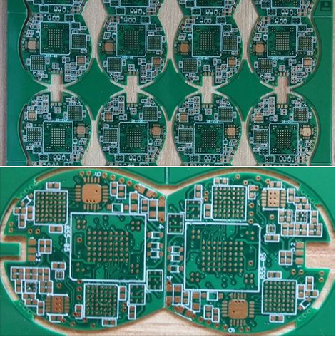
Mastering High Frequency PCB Connections For Seamless Data Transfer
In today's fast-paced digital world, seamless data transfer is critical for applications ranging from telecommunications to high-speed computing. At the heart of these systems lies the printed circuit board (PCB), which facilitates the efficient transmission of high-frequency signals. Mastering high-frequency PCB connections is essential to ensure minimal signal loss, reduced interference, and optimal performance. This article delves into the key aspects of designing and implementing high-frequency PCB connections, providing insights into the techniques and considerations that engineers must address to achieve flawless data transfer.
Understanding High-Frequency PCB Design
High-frequency PCB design differs significantly from traditional PCB layouts due to the unique challenges posed by rapid signal transitions. At high frequencies, signals are more susceptible to losses, reflections, and electromagnetic interference (EMI). To mitigate these issues, engineers must carefully consider the materials, trace geometries, and layer stack-ups used in the PCB.
One critical factor is the dielectric constant (Dk) of the substrate material. Materials with a stable Dk over a wide frequency range, such as Rogers or Teflon, are often preferred for high-frequency applications. Additionally, the thickness of the dielectric layer and the copper traces must be optimized to maintain consistent impedance and reduce signal degradation.
Impedance Matching and Signal Integrity
Impedance matching is paramount in high-frequency PCB design to prevent signal reflections and ensure efficient power transfer. Mismatched impedance can lead to standing waves, which degrade signal quality and cause data errors. To achieve proper impedance matching, engineers must calculate the characteristic impedance of transmission lines and design traces accordingly.
Microstrip and stripline configurations are commonly used for high-frequency traces. Microstrip traces are routed on the outer layers of the PCB, while stripline traces are embedded between ground planes. Each configuration has its advantages, with microstrips offering easier access for debugging and striplines providing better EMI shielding. The choice depends on the specific requirements of the application.
Minimizing Crosstalk and EMI
Crosstalk and electromagnetic interference (EMI) are major concerns in high-frequency PCB designs. Crosstalk occurs when signals from one trace interfere with adjacent traces, leading to data corruption. To minimize crosstalk, engineers must maintain adequate spacing between traces and use ground planes to isolate sensitive signals.
EMI can radiate from the PCB and interfere with other electronic devices, or external EMI can disrupt the PCB's operation. Shielding techniques, such as using grounded metal enclosures or adding EMI filters, are effective in reducing interference. Additionally, careful routing of high-speed signals away from noisy components and power lines can further enhance EMI performance.
Advanced Techniques for High-Frequency PCBs
As data rates continue to rise, advanced techniques such as differential signaling and via optimization become essential. Differential signaling involves transmitting signals over paired traces with opposite polarities, which improves noise immunity and reduces EMI. This technique is widely used in high-speed interfaces like USB, HDMI, and PCIe.
Vias, which connect different layers of the PCB, can introduce impedance discontinuities and signal loss at high frequencies. To address this, engineers use techniques like back-drilling to remove unused via stubs and via-in-pad designs to minimize parasitic capacitance. These methods help maintain signal integrity and ensure reliable data transfer.
Testing and Validation
Thorough testing and validation are crucial to ensuring the performance of high-frequency PCBs. Time-domain reflectometry (TDR) is commonly used to measure impedance and identify discontinuities in transmission lines. Vector network analyzers (VNAs) can assess the frequency response of the PCB and detect losses or resonances.
Simulation tools, such as SPICE or 3D electromagnetic simulators, allow engineers to model and optimize their designs before fabrication. By combining simulation with physical testing, designers can identify and rectify potential issues early in the development process, saving time and costs.
Mastering high-frequency PCB connections requires a deep understanding of signal integrity, material properties, and advanced design techniques. By addressing these challenges, engineers can create PCBs that deliver seamless data transfer, meeting the demands of modern high-speed applications.

Cutting Edge High Frequency Signal Transmission PCB Technologies
In today's fast-paced technological landscape, the demand for high-frequency signal transmission has skyrocketed, driven by advancements in telecommunications, aerospace, and consumer electronics. At the heart of this revolution lies Cutting Edge High Frequency Signal Transmission PCB Technologies, a field that is redefining how we design and manufacture printed circuit boards (PCBs) to handle ultra-high frequencies with minimal loss and interference. These technologies are critical for applications like 5G networks, satellite communications, and high-speed data processing, where signal integrity is paramount. This article delves into the innovative techniques and materials that are pushing the boundaries of what PCBs can achieve.
Advanced Materials for High-Frequency PCBs
One of the cornerstones of high-frequency PCB technology is the use of advanced materials. Traditional FR4 substrates, while cost-effective, are inadequate for high-frequency applications due to their high dielectric loss and inconsistent performance at elevated frequencies. Instead, materials like Rogers, Teflon, and ceramic-filled laminates are now preferred. These materials exhibit low dielectric constants and dissipation factors, ensuring minimal signal loss and distortion.
Moreover, these advanced materials offer superior thermal stability, which is crucial for maintaining performance in harsh environments. For instance, aerospace applications require PCBs that can withstand extreme temperatures and radiation. The integration of these materials into PCB manufacturing has opened new possibilities for high-frequency designs, enabling faster and more reliable signal transmission.
Precision Design and Manufacturing Techniques
Designing PCBs for high-frequency signals requires meticulous attention to detail. Signal integrity is highly dependent on factors like trace width, spacing, and layer stacking. Engineers use sophisticated software tools to simulate and optimize these parameters before production. Techniques such as controlled impedance routing and differential pair routing are employed to minimize crosstalk and electromagnetic interference (EMI).
Manufacturing these PCBs also demands precision. Laser drilling and photolithography are used to create fine traces and vias, ensuring minimal signal distortion. Additionally, surface finishes like gold or silver are applied to reduce resistance and improve conductivity. The combination of advanced design and manufacturing techniques ensures that high-frequency PCBs meet the stringent requirements of modern applications.
Innovative Shielding and Grounding Strategies
High-frequency signals are particularly susceptible to interference, making shielding and grounding critical aspects of PCB design. Engineers employ various strategies to isolate sensitive signals from noise sources. For example, ground planes are strategically placed to provide a low-impedance return path, reducing EMI. Shielding cans and conductive coatings are also used to encapsulate high-frequency components, preventing external interference.
Another innovative approach is the use of buried capacitance and inductance within the PCB layers. These embedded passive components help filter out noise and stabilize power delivery, further enhancing signal integrity. By integrating these shielding and grounding techniques, high-frequency PCBs can achieve unparalleled performance in noisy environments.
Future Trends and Challenges
The field of high-frequency PCB technology is continuously evolving, with researchers exploring new materials and techniques to push the limits further. For instance, the development of graphene-based substrates promises even lower dielectric losses and higher thermal conductivity. Similarly, 3D printing technologies are being investigated for their potential to create complex, high-frequency PCB structures with unprecedented precision.
However, challenges remain. The high cost of advanced materials and manufacturing processes can be a barrier to widespread adoption. Additionally, as frequencies continue to rise, new issues like skin effect and dielectric heating become more pronounced. Addressing these challenges will require ongoing innovation and collaboration across the industry.
In conclusion, Cutting Edge High Frequency Signal Transmission PCB Technologies are paving the way for the next generation of electronic devices. By leveraging advanced materials, precision design, and innovative shielding techniques, these technologies are enabling faster, more reliable signal transmission in an increasingly connected world.

High Speed Signal Transmission PCB Techniques And Innovations
In today's fast-paced digital world, the demand for high-speed signal transmission has never been greater. From data centers to consumer electronics, the ability to transmit signals quickly and reliably is critical for performance and efficiency. High Speed Signal Transmission PCB Techniques And Innovations explores the cutting-edge technologies and methodologies that enable printed circuit boards (PCBs) to handle these high-speed signals effectively. This article delves into the latest advancements, materials, and design strategies that are revolutionizing the field, offering engineers and designers valuable insights into optimizing their PCB designs for high-speed applications.
Material Innovations for High-Speed PCBs
The choice of materials plays a pivotal role in the performance of high-speed PCBs. Traditional materials like FR4 are often insufficient for high-frequency applications due to their dielectric properties. Advanced materials such as Rogers, Teflon, and Isola offer lower dielectric constants and dissipation factors, which are essential for minimizing signal loss and maintaining signal integrity.
Moreover, the development of hybrid materials combines the benefits of different substrates to achieve optimal performance. For instance, a hybrid PCB might use a high-speed material for critical signal layers and a cost-effective material for less critical layers. This approach not only enhances performance but also helps in managing costs, making it a popular choice among designers.
Impedance Control and Signal Integrity
Maintaining consistent impedance is crucial for high-speed signal transmission. Variations in impedance can lead to signal reflections, which degrade signal quality and cause errors. To address this, designers employ techniques such as controlled impedance routing and the use of differential pairs.
Controlled impedance routing involves carefully calculating the trace width, spacing, and layer stack-up to achieve the desired impedance. Differential pairs, on the other hand, are used to transmit high-speed signals as complementary pairs, which helps in canceling out noise and improving signal integrity. These techniques are essential for ensuring reliable high-speed communication.
Advanced Routing Techniques
Routing high-speed signals requires meticulous planning to avoid issues like crosstalk and electromagnetic interference (EMI). One common approach is to use microstrip and stripline routing configurations. Microstrip routing places the signal trace on an outer layer with a ground plane beneath, while stripline routing embeds the trace between two ground planes, offering better EMI shielding.
Another innovative technique is the use of via stitching and ground vias to minimize return path discontinuities. By strategically placing vias around high-speed traces, designers can ensure a low-impedance return path, reducing noise and improving signal quality. These advanced routing techniques are vital for achieving optimal performance in high-speed PCBs.
Power Integrity and Decoupling
Power integrity is often overlooked but is equally important for high-speed signal transmission. Fluctuations in power supply can introduce noise, affecting signal quality. To mitigate this, designers use decoupling capacitors to stabilize the power supply and filter out high-frequency noise.
Additionally, proper power plane design is essential. Splitting power planes and using multiple vias to connect them can help in reducing inductance and ensuring a stable power delivery network. These practices are critical for maintaining signal integrity and overall system performance.
Simulation and Testing
Before manufacturing, simulating high-speed PCB designs is a crucial step to identify potential issues. Tools like SPICE, HyperLynx, and ADS allow designers to analyze signal integrity, power integrity, and EMI performance. These simulations help in optimizing the design and avoiding costly revisions.
Post-manufacturing testing is equally important. Techniques like time-domain reflectometry (TDR) and vector network analysis (VNA) are used to validate the performance of high-speed PCBs. These tests ensure that the final product meets the required specifications and performs reliably in real-world applications.
In conclusion, High Speed Signal Transmission PCB Techniques And Innovations encompass a wide range of strategies and technologies aimed at optimizing PCB performance. From material selection to advanced routing and rigorous testing, each aspect plays a vital role in ensuring reliable high-speed signal transmission. As technology continues to evolve, staying abreast of these innovations is essential for engineers and designers striving to push the boundaries of what's possible.
REPORT

