-
 Agriculture
-
 Health-Care
-
 Environment
-
 Construction-Real-Estate
-
 Tools-Hardware
-
 Home-Garden
-
 Furniture
-
 Luggage-Bags-Cases
-
 Medical-devices-Supplies
-
 Gifts-Crafts
-
 Sports-Entertainment
-
 Food-Beverage
-
 Vehicles-Transportation
-
 Power-Transmission
-
 Material-Handling
-
 Renewable-Energy
-
 Safety
-
 Testing-Instrument-Equipment
-
 Construction-Building-Machinery
-
 Pet-Supplies
-
 Personal-Care-Household-Cleaning
-
 Vehicle-Accessories-Electronics-Tools
-
 School-Office-Supplies
-
 Packaging-Printing
-
 Mother-Kids-Toys
-
 Business-Services
-
 Commercial-Equipment-Machinery
-
 Apparel-Accessories
-
 Security
-
 Shoes-Accessories
-
 Vehicle-Parts-Accessories
-
 Jewelry-Eyewear-Watches-Accessories
-
 Lights-Lighting
-
 Fabric-Textile-Raw-Material
-
 Fabrication-Services
-
 Industrial-Machinery
-
 Consumer-Electronics
-
 Electrical-Equipment-Supplies
-
 Electronic-Components-Accessories-Telecommunications
-
 Home-Appliances
-
 Beauty
-
 Chemicals
-
 Rubber-Plastics
-
 Metals-Alloys
- Masonry Materials
- Curtain Walls & Accessories
- Earthwork Products
- Fireproofing Materials
- Heat Insulation Materials
- Plastic Building Materials
- Building Boards
- Soundproofing Materials
- Timber
- Waterproofing Materials
- Balustrades & Handrails
- Bathroom & Kitchen
- Flooring & Accessories
- Tiles & Accessories
- Door, Window & Accessories
- Fireplaces & Stoves
- Floor Heating Systems & Parts
- Stairs & Stair Parts
- Ceilings
- Elevators & Escalators
- Stone
- Countertops, Vanity Tops & Table Tops
- Mosaics
- Metal Building Materials
- Multifunctional Materials
- Ladders & Scaffoldings
- Mouldings
- Corner Guards
- Decorative Films
- Formwork
- Building & Industrial Glass
- Other Construction & Real Estate
- Wallpapers/Wall panels
- HVAC System & Parts
- Outdoor Facilities
- Prefabricated Buildings
- Festive & Party Supplies
- Bathroom Products
- Household Sundries
- Rain Gear
- Garden Supplies
- Household Cleaning Tools & Accessories
- Lighters & Smoking Accessories
- Home Storage & Organization
- Household Scales
- Smart Home Improvement
- Home Textiles
- Kitchenware
- Drinkware & Accessories
- Dinnerware, Coffee & Wine
- Home Decor
- Golf
- Fitness & Body Building
- Amusement Park Facilities
- Billiards, Board Game,Coin Operated Games
- Musical Instruments
- Outdoor Affordable Luxury Sports
- Camping & Hiking
- Fishing
- Sports Safety&Rehabilitation
- Ball Sports Equipments
- Water Sports
- Winter Sports
- Luxury Travel Equipments
- Sports Shoes, Bags & Accessories
- Cycling
- Other Sports & Entertainment Products
- Artificial Grass&Sports Flooring&Sports Court Equipment
- Scooters
- Food Ingredients
- Honey & Honey Products
- Snacks
- Nuts & Kernels
- Seafood
- Plant & Animal Oil
- Beverages
- Fruit & Vegetable Products
- Frog & Escargot
- Bean Products
- Egg Products
- Dairy Products
- Seasonings & Condiments
- Canned Food
- Instant Food
- Baked Goods
- Other Food & Beverage
- Meat & Poultry
- Confectionery
- Grain Products
- Feminie Care
- Hair Care & Styling
- Body Care
- Hands & Feet Care
- Hygiene Products
- Men's Grooming
- Laundry Cleaning Supplies
- Travel Size & Gift Sets
- Room Deodorizers
- Other Personal Care Products
- Pest Control Products
- Special Household Cleaning
- Floor Cleaning
- Kitchen & Bathroom Cleaning
- Oral Care
- Bath Supplies
- Yellow Pages
- Correction Supplies
- Office Binding Supplies
- Office Cutting Supplies
- Board Erasers
- Office Adhesives & Tapes
- Education Supplies
- Pencil Cases & Bags
- Notebooks & Writing Pads
- File Folder Accessories
- Calendars
- Writing Accessories
- Commercial Office Supplies
- Pencil Sharpeners
- Pens
- Letter Pad/Paper
- Paper Envelopes
- Desk Organizers
- Pencils
- Markers & Highlighters
- Filing Products
- Art Supplies
- Easels
- Badge Holder & Accessories
- Office Paper
- Printer Supplies
- Book Covers
- Other Office & School Supplies
- Stationery Set
- Boards
- Clipboards
- Stamps
- Drafting Supplies
- Stencils
- Electronic Dictionary
- Books
- Map
- Magazines
- Calculators
- Baby & Toddler Toys
- Educational Toys
- Classic Toys
- Dress Up & Pretend Play
- Toy Vehicle
- Stuffed Animals & Plush Toys
- Outdoor Toys & Structures
- Balloons & Accessories
- Baby Food
- Children's Clothing
- Baby Supplies & Products
- Maternity Clothes
- Kids Shoes
- Baby Care
- Novelty & Gag Toys
- Dolls & Accessories
- Puzzle & Games
- Blocks & Model Building Toys
- Toddler Clothing
- Baby Clothing
- Kids' Luggage & Bags
- Arts, Crafts & DIY Toys
- Action & Toy Figures
- Baby Appliances
- Hobbies & Models
- Remote Control Toys
- Promotional Toys
- Pregnancy & Maternity
- Hygiene Products
- Kid's Textile&Bedding
- Novelty & Special Use
- Toy Weapons
- Baby Gifts
- Baby Storage & Organization
- Auto Drive Systems
- ATV/UTV Parts & Accessories
- Marine Parts & Accessories
- Other Auto Parts
- Trailer Parts & Accessories
- Auto Transmission Systems
- Train Parts & Accessories
- Universal Parts
- Railway Parts & Accessories
- Auto Brake Systems
- Aviation Parts & Accessories
- Truck Parts & Accessories
- Auto Suspension Systems
- Auto Lighting Systems
- New Energy Vehicle Parts & Accessories
- Auto Steering Systems
- Wheels, Tires & Accessories
- Bus Parts & Accessories
- Auto Performance Parts
- Cooling System
- Go-Kart & Kart Racer Parts & Accessories
- Air Conditioning Systems
- Heavy Duty Vehicle Parts & Accessories
- Auto Electrical Systems
- Auto Body Systems
- Auto Engine Systems
- Container Parts & Accessories
- Motorcycle Parts & Accessories
- Refrigeration & Heat Exchange Equipment
- Machine Tool Equipment
- Food & Beverage Machinery
- Agricultural Machinery & Equipment
- Apparel & Textile Machinery
- Chemical Machinery
- Packaging Machines
- Paper Production Machinery
- Plastic & Rubber Processing Machinery
- Industrial Robots
- Electronic Products Machinery
- Metal & Metallurgy Machinery
- Woodworking Machinery
- Home Product Manufacturing Machinery
- Machinery Accessories
- Environmental Machinery
- Machinery Service
- Electrical Equipment Manufacturing Machinery
- Industrial Compressors & Parts
- Tobacco & Cigarette Machinery
- Production Line
- Used Industrial Machinery
- Electronics Production Machinery
- Other Machinery & Industrial Equipment
- Camera, Photo & Accessories
- Portable Audio, Video & Accessories
- Television, Home Audio, Video & Accessories
- Video Games & Accessories
- Mobile Phone & Accessories
- Electronic Publications
- Earphone & Headphone & Accessories
- Speakers & Accessories
- Smart Electronics
- TV Receivers & Accessories
- Mobile Phone & Computer Repair Parts
- Chargers, Batteries & Power Supplies
- Used Electronics
- VR, AR, MR Hardware & Software
- Projectors & Presentation Equipments
- Other Consumer Electronics
- Cables & Commonly Used Accessories
- Computer Hardware & Software
- Displays, Signage and Optoelectronics
- Discrete Semiconductors
- Wireless & IoT Module and Products
- Telecommunications
- Connectors, Terminals & Accessories
- Development Boards, Electronic Modules and Kits
- Circuit Protection
- Sensors
- Isolators
- Audio Components and Products
- Integrated Circuits
- Power Supplies
- Relays
- RF, Microwave and RFID
- Electronic Accessories & Supplies
- Passive Components
- PCB & PCBA
- Air Quality Appliances
- Home Appliance Parts
- Heating & Cooling Appliances
- Small Kitchen Appliances
- Laundry Appliances
- Water Heaters
- Water Treatment Appliances
- Refrigerators & Freezers
- Personal Care & Beauty Appliances
- Major Kitchen Appliances
- Cleaning Appliances
- Second-hand Appliances
- Smart Home Appliances
- Other Home Appliances
- Energy Chemicals
- Inorganic Chemicals
- Basic Organic Chemicals
- Agrochemicals
- Admixture & Additives
- Catalysts & Chemical Auxiliary Agents
- Pigments & Dyestuff
- Coating & Paint
- Daily Chemicals
- Polymer
- Organic Intermediate
- Adhesives & Sealants
- Chemical Waste
- Biological Chemical Products
- Surface Treatment Chemicals
- Painting & Coating
- Chemical Reagents
- Flavor & Fragrance
- Non-Explosive Demolition Agents
- Other Chemicals
- Custom Chemical Services
Wireless & IoT Module and Products
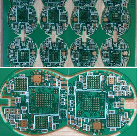
Achieving Micron Level Accuracy with High Precision PCB Deep Hole Control
In the rapidly evolving world of electronics manufacturing, precision is paramount. One of the most critical aspects of producing high-quality printed circuit boards (PCBs) is achieving micron-level accuracy in deep hole control. This process ensures that the intricate layers of a PCB align perfectly, enabling the seamless integration of components and the reliable performance of electronic devices. As devices become smaller and more complex, the demand for high-precision PCB manufacturing has never been higher. This article delves into the techniques and technologies that make achieving micron-level accuracy possible, offering insights into the challenges and innovations in this field.
The Importance of Micron-Level Accuracy in PCB Manufacturing
Micron-level accuracy is essential for modern PCBs, which often feature densely packed components and multi-layer designs. Even the slightest deviation in hole placement or diameter can lead to misalignment, electrical shorts, or complete circuit failure. High-precision deep hole control ensures that vias, through-holes, and microvias are drilled with exceptional accuracy, maintaining the integrity of the PCB's electrical pathways.
Moreover, as the industry moves toward miniaturization, the tolerances for error are shrinking. Devices such as smartphones, medical implants, and aerospace electronics require PCBs with holes drilled to within a few microns of their specified dimensions. Achieving this level of precision is not just a technical challenge but also a competitive advantage for manufacturers.
Advanced Drilling Technologies for High Precision
To achieve micron-level accuracy, manufacturers rely on advanced drilling technologies such as laser drilling and mechanical drilling with ultra-precise spindles. Laser drilling, in particular, offers unparalleled precision by using focused laser beams to create holes as small as 10 microns in diameter. This method is especially useful for creating microvias in high-density interconnect (HDI) PCBs.
Mechanical drilling, on the other hand, has also seen significant advancements. High-speed spindles with minimal runout and advanced drill bits coated with diamond-like carbon (DLC) can achieve tolerances of ±5 microns. These technologies are complemented by real-time monitoring systems that adjust drilling parameters on the fly to compensate for tool wear or material inconsistencies.
Material Considerations for Deep Hole Control
The materials used in PCB manufacturing play a crucial role in achieving high-precision deep hole control. Traditional materials like FR-4 are being supplemented by high-performance laminates such as polyimide and PTFE, which offer better thermal stability and dimensional accuracy. These materials reduce the risk of deformation during drilling, ensuring that holes maintain their intended dimensions.
Additionally, the choice of copper foil thickness and the use of laser-direct imaging (LDI) for patterning can influence hole accuracy. Thinner copper foils reduce the risk of drill bit deflection, while LDI ensures that the patterns are aligned with the drilled holes, further enhancing precision.
Quality Control and Inspection Techniques
Ensuring micron-level accuracy requires rigorous quality control and inspection techniques. Automated optical inspection (AOI) systems are used to scan PCBs for any deviations in hole placement or diameter. These systems can detect defects as small as a few microns, allowing manufacturers to correct issues before they escalate.
X-ray inspection is another critical tool, particularly for multi-layer PCBs. It allows manufacturers to inspect the internal layers of the board without destructive testing, ensuring that all holes are perfectly aligned and free of defects. Together, these inspection methods provide a comprehensive quality assurance process.
Future Trends in High-Precision PCB Manufacturing
The future of high-precision PCB manufacturing lies in the integration of artificial intelligence (AI) and machine learning (ML). These technologies can analyze vast amounts of data from the drilling process to identify patterns and optimize parameters in real time. This not only improves accuracy but also reduces waste and increases production efficiency.
Another emerging trend is the use of additive manufacturing techniques, such as 3D printing, to create PCBs with complex geometries and ultra-fine features. While still in its early stages, this approach has the potential to revolutionize the industry by enabling even greater precision and design flexibility.
In conclusion, achieving micron-level accuracy in PCB deep hole control is a multifaceted challenge that requires advanced technologies, careful material selection, and stringent quality control. As the demand for smaller and more complex electronic devices grows, manufacturers must continue to innovate to meet these exacting standards.

High Precision PCB Deep Hole Management for Enhanced Electrical Connectivity
In the rapidly evolving world of electronics, the demand for high-performance printed circuit boards (PCBs) has never been greater. One critical aspect of PCB manufacturing that significantly impacts electrical connectivity is deep hole management. High Precision PCB Deep Hole Management for Enhanced Electrical Connectivity is a cutting-edge approach that ensures reliable signal transmission, minimizes signal loss, and improves overall circuit performance. This article delves into the importance of deep hole management, its challenges, and the innovative techniques used to achieve precision in modern PCB designs.
PCBs are the backbone of electronic devices, and their functionality relies heavily on the quality of vias—tiny holes that connect different layers of the board. Deep holes, or high-aspect-ratio vias, are particularly challenging due to their depth and narrow diameter. Poorly managed deep holes can lead to electrical discontinuities, increased resistance, and even circuit failure. As electronic devices become more compact and complex, mastering deep hole management has become essential for ensuring enhanced electrical connectivity and device reliability.
The Importance of High Precision in Deep Hole Management
High precision in deep hole management is crucial for maintaining the integrity of electrical connections in multi-layer PCBs. As devices shrink in size but grow in functionality, the need for densely packed circuits with reliable interconnects has skyrocketed. Deep holes must be drilled with extreme accuracy to ensure proper plating and avoid issues like misalignment or incomplete conduction paths.
Moreover, high precision directly impacts signal integrity. In high-frequency applications, even minor imperfections in deep holes can cause signal reflections, crosstalk, and attenuation. By employing advanced drilling and plating techniques, manufacturers can achieve the level of precision required for today’s high-speed and high-frequency PCB designs.
Challenges in Deep Hole Drilling and Plating
Drilling deep holes with high aspect ratios presents several technical challenges. Traditional drilling methods often struggle to maintain consistency in hole diameter and wall smoothness, especially as the depth increases. Any deviation can lead to uneven plating, which compromises electrical connectivity.
Plating deep holes is another significant hurdle. Ensuring uniform copper deposition throughout the hole’s depth is critical for reliable conductivity. However, achieving this uniformity is difficult due to factors like electrolyte flow restrictions and varying current densities. Innovative plating techniques, such as pulse plating and vacuum deposition, have been developed to address these challenges and enhance plating quality.
Advanced Techniques for Precision Deep Hole Management
To overcome the challenges associated with deep hole management, manufacturers have adopted several advanced techniques. Laser drilling, for instance, offers unparalleled precision and control, enabling the creation of microvias with extremely high aspect ratios. This method minimizes thermal damage and ensures cleaner hole walls, which are essential for subsequent plating processes.
Another breakthrough is the use of additive manufacturing for PCB fabrication. 3D printing technologies allow for the creation of complex via structures with precise dimensions, reducing the risk of defects. Additionally, electroplating advancements, such as direct current (DC) and periodic pulse reverse (PPR) plating, have improved copper deposition uniformity in deep holes.
The Role of Materials in Enhancing Electrical Connectivity
The choice of materials plays a pivotal role in deep hole management and electrical connectivity. High-quality dielectric materials with low thermal expansion coefficients ensure dimensional stability during drilling and plating processes. Similarly, using high-purity copper for plating reduces resistivity and enhances signal transmission.
Innovative materials like conductive inks and polymers are also being explored to simplify the plating process and improve performance. These materials can be applied selectively, reducing waste and enabling more efficient production of high-density interconnects (HDIs).
Future Trends in PCB Deep Hole Management
The future of PCB deep hole management lies in further miniaturization and automation. As the Internet of Things (IoT) and 5G technologies continue to expand, the demand for ultra-high-density PCBs will grow. This will drive the development of even more precise drilling and plating technologies, such as femtosecond laser drilling and atomic layer deposition (ALD).
Additionally, artificial intelligence (AI) and machine learning (ML) are expected to play a significant role in optimizing deep hole management processes. These technologies can analyze vast amounts of data to identify patterns and predict potential defects, enabling proactive quality control and reducing production costs.
In conclusion, High Precision PCB Deep Hole Management for Enhanced Electrical Connectivity is a vital aspect of modern electronics manufacturing. By addressing the challenges and leveraging advanced techniques, manufacturers can ensure reliable, high-performance PCBs that meet the demands of tomorrow’s technology.

High Precision PCB Deep Hole Control Solutions for Reliable Circuit Performance
In the rapidly evolving world of electronics, the demand for high-performance printed circuit boards (PCBs) has never been greater. One critical aspect of PCB manufacturing that directly impacts reliability and performance is the precision control of deep holes. High Precision PCB Deep Hole Control Solutions for Reliable Circuit Performance addresses this vital need, ensuring that modern electronic devices meet stringent quality standards. As PCBs become more complex and miniaturized, the accuracy of deep hole drilling—used for vias, through-holes, and other interconnects—plays a pivotal role in signal integrity, thermal management, and overall circuit functionality. This article explores the cutting-edge solutions that enable manufacturers to achieve unparalleled precision in deep hole control, ultimately enhancing the reliability of electronic systems.
The Importance of Deep Hole Precision in PCBs
Deep holes in PCBs serve as conduits for electrical connections between different layers of the board. These holes, often referred to as vias or through-holes, must be drilled with extreme accuracy to ensure proper alignment and conductivity. Any deviation in hole placement or diameter can lead to signal loss, short circuits, or even complete board failure. High-precision deep hole control solutions mitigate these risks by leveraging advanced drilling technologies and real-time monitoring systems.
Moreover, as electronic devices shrink in size but grow in functionality, the density of components on PCBs increases. This trend necessitates smaller and more precisely drilled holes, often with aspect ratios that challenge traditional drilling methods. High-precision solutions address these challenges by incorporating laser drilling, mechanical drilling with ultra-fine bits, and computer-controlled positioning systems that operate at micron-level tolerances.
Advanced Technologies for High-Precision Deep Hole Drilling
One of the most significant advancements in deep hole drilling is the adoption of laser drilling technology. Lasers offer unparalleled precision, capable of creating holes as small as a few microns in diameter. This method is particularly beneficial for high-density interconnect (HDI) PCBs, where traditional mechanical drills may struggle with the required accuracy. Laser drilling also minimizes thermal damage to surrounding materials, preserving the integrity of the PCB.
Another key technology is computer numerical control (CNC) drilling machines equipped with high-speed spindles and adaptive control systems. These machines use real-time feedback to adjust drilling parameters dynamically, ensuring consistent hole quality across the entire board. Additionally, the integration of vision systems and automated alignment tools further enhances precision by compensating for any material shifts or distortions during the drilling process.
Quality Control and Inspection Techniques
Ensuring the accuracy of deep holes doesn’t end with drilling; rigorous quality control measures are essential. Automated optical inspection (AOI) systems are widely used to verify hole placement, diameter, and depth. These systems employ high-resolution cameras and sophisticated software to detect even the slightest deviations from design specifications.
Another critical inspection technique is X-ray imaging, which allows manufacturers to examine the internal structure of vias and through-holes. This non-destructive testing method is particularly useful for multilayer PCBs, where hidden defects could compromise performance. By combining these inspection methods with statistical process control (SPC), manufacturers can maintain tight tolerances and reduce the risk of defects.
Material Considerations for Deep Hole Drilling
The choice of materials significantly impacts the success of deep hole drilling in PCBs. For instance, the glass transition temperature (Tg) of the substrate material affects its stability during drilling. High-Tg materials are preferred for their ability to withstand the heat generated during the drilling process without deforming.
Additionally, the copper plating inside the holes must be uniform to ensure reliable electrical connections. Advanced electroplating techniques, such as pulse plating, help achieve consistent copper deposition, even in high-aspect-ratio holes. Manufacturers must also consider the dielectric properties of the PCB material, as these influence signal integrity and thermal management.
Future Trends in High-Precision Deep Hole Control
The future of high-precision deep hole control lies in the continued integration of artificial intelligence (AI) and machine learning (ML) into manufacturing processes. AI-powered systems can analyze vast amounts of data from drilling and inspection processes to identify patterns and optimize parameters in real time. This capability will further enhance precision and reduce waste.
Another emerging trend is the use of additive manufacturing techniques, such as 3D printing, to create PCBs with embedded vias and complex geometries. While still in its early stages, this approach has the potential to revolutionize PCB design and manufacturing by enabling structures that are impossible to achieve with traditional subtractive methods.
As the electronics industry continues to push the boundaries of miniaturization and performance, high-precision deep hole control solutions will remain a cornerstone of reliable PCB manufacturing. By embracing advanced technologies and rigorous quality control measures, manufacturers can meet the ever-growing demands of modern electronic devices.
REPORT

