-
 Agriculture
-
 Health-Care
-
 Environment
-
 Construction-Real-Estate
-
 Tools-Hardware
-
 Home-Garden
-
 Furniture
-
 Luggage-Bags-Cases
-
 Medical-devices-Supplies
-
 Gifts-Crafts
-
 Sports-Entertainment
-
 Food-Beverage
-
 Vehicles-Transportation
-
 Power-Transmission
-
 Material-Handling
-
 Renewable-Energy
-
 Safety
-
 Testing-Instrument-Equipment
-
 Construction-Building-Machinery
-
 Pet-Supplies
-
 Personal-Care-Household-Cleaning
-
 Vehicle-Accessories-Electronics-Tools
-
 School-Office-Supplies
-
 Packaging-Printing
-
 Mother-Kids-Toys
-
 Business-Services
-
 Commercial-Equipment-Machinery
-
 Apparel-Accessories
-
 Security
-
 Shoes-Accessories
-
 Vehicle-Parts-Accessories
-
 Jewelry-Eyewear-Watches-Accessories
-
 Lights-Lighting
-
 Fabric-Textile-Raw-Material
-
 Fabrication-Services
-
 Industrial-Machinery
-
 Consumer-Electronics
-
 Electrical-Equipment-Supplies
-
 Electronic-Components-Accessories-Telecommunications
-
 Home-Appliances
-
 Beauty
-
 Chemicals
-
 Rubber-Plastics
-
 Metals-Alloys
- Masonry Materials
- Curtain Walls & Accessories
- Earthwork Products
- Fireproofing Materials
- Heat Insulation Materials
- Plastic Building Materials
- Building Boards
- Soundproofing Materials
- Timber
- Waterproofing Materials
- Balustrades & Handrails
- Bathroom & Kitchen
- Flooring & Accessories
- Tiles & Accessories
- Door, Window & Accessories
- Fireplaces & Stoves
- Floor Heating Systems & Parts
- Stairs & Stair Parts
- Ceilings
- Elevators & Escalators
- Stone
- Countertops, Vanity Tops & Table Tops
- Mosaics
- Metal Building Materials
- Multifunctional Materials
- Ladders & Scaffoldings
- Mouldings
- Corner Guards
- Decorative Films
- Formwork
- Building & Industrial Glass
- Other Construction & Real Estate
- Wallpapers/Wall panels
- HVAC System & Parts
- Outdoor Facilities
- Prefabricated Buildings
- Festive & Party Supplies
- Bathroom Products
- Household Sundries
- Rain Gear
- Garden Supplies
- Household Cleaning Tools & Accessories
- Lighters & Smoking Accessories
- Home Storage & Organization
- Household Scales
- Smart Home Improvement
- Home Textiles
- Kitchenware
- Drinkware & Accessories
- Dinnerware, Coffee & Wine
- Home Decor
- Golf
- Fitness & Body Building
- Amusement Park Facilities
- Billiards, Board Game,Coin Operated Games
- Musical Instruments
- Outdoor Affordable Luxury Sports
- Camping & Hiking
- Fishing
- Sports Safety&Rehabilitation
- Ball Sports Equipments
- Water Sports
- Winter Sports
- Luxury Travel Equipments
- Sports Shoes, Bags & Accessories
- Cycling
- Other Sports & Entertainment Products
- Artificial Grass&Sports Flooring&Sports Court Equipment
- Scooters
- Food Ingredients
- Honey & Honey Products
- Snacks
- Nuts & Kernels
- Seafood
- Plant & Animal Oil
- Beverages
- Fruit & Vegetable Products
- Frog & Escargot
- Bean Products
- Egg Products
- Dairy Products
- Seasonings & Condiments
- Canned Food
- Instant Food
- Baked Goods
- Other Food & Beverage
- Meat & Poultry
- Confectionery
- Grain Products
- Feminie Care
- Hair Care & Styling
- Body Care
- Hands & Feet Care
- Hygiene Products
- Men's Grooming
- Laundry Cleaning Supplies
- Travel Size & Gift Sets
- Room Deodorizers
- Other Personal Care Products
- Pest Control Products
- Special Household Cleaning
- Floor Cleaning
- Kitchen & Bathroom Cleaning
- Oral Care
- Bath Supplies
- Yellow Pages
- Correction Supplies
- Office Binding Supplies
- Office Cutting Supplies
- Board Erasers
- Office Adhesives & Tapes
- Education Supplies
- Pencil Cases & Bags
- Notebooks & Writing Pads
- File Folder Accessories
- Calendars
- Writing Accessories
- Commercial Office Supplies
- Pencil Sharpeners
- Pens
- Letter Pad/Paper
- Paper Envelopes
- Desk Organizers
- Pencils
- Markers & Highlighters
- Filing Products
- Art Supplies
- Easels
- Badge Holder & Accessories
- Office Paper
- Printer Supplies
- Book Covers
- Other Office & School Supplies
- Stationery Set
- Boards
- Clipboards
- Stamps
- Drafting Supplies
- Stencils
- Electronic Dictionary
- Books
- Map
- Magazines
- Calculators
- Baby & Toddler Toys
- Educational Toys
- Classic Toys
- Dress Up & Pretend Play
- Toy Vehicle
- Stuffed Animals & Plush Toys
- Outdoor Toys & Structures
- Balloons & Accessories
- Baby Food
- Children's Clothing
- Baby Supplies & Products
- Maternity Clothes
- Kids Shoes
- Baby Care
- Novelty & Gag Toys
- Dolls & Accessories
- Puzzle & Games
- Blocks & Model Building Toys
- Toddler Clothing
- Baby Clothing
- Kids' Luggage & Bags
- Arts, Crafts & DIY Toys
- Action & Toy Figures
- Baby Appliances
- Hobbies & Models
- Remote Control Toys
- Promotional Toys
- Pregnancy & Maternity
- Hygiene Products
- Kid's Textile&Bedding
- Novelty & Special Use
- Toy Weapons
- Baby Gifts
- Baby Storage & Organization
- Auto Drive Systems
- ATV/UTV Parts & Accessories
- Marine Parts & Accessories
- Other Auto Parts
- Trailer Parts & Accessories
- Auto Transmission Systems
- Train Parts & Accessories
- Universal Parts
- Railway Parts & Accessories
- Auto Brake Systems
- Aviation Parts & Accessories
- Truck Parts & Accessories
- Auto Suspension Systems
- Auto Lighting Systems
- New Energy Vehicle Parts & Accessories
- Auto Steering Systems
- Wheels, Tires & Accessories
- Bus Parts & Accessories
- Auto Performance Parts
- Cooling System
- Go-Kart & Kart Racer Parts & Accessories
- Air Conditioning Systems
- Heavy Duty Vehicle Parts & Accessories
- Auto Electrical Systems
- Auto Body Systems
- Auto Engine Systems
- Container Parts & Accessories
- Motorcycle Parts & Accessories
- Refrigeration & Heat Exchange Equipment
- Machine Tool Equipment
- Food & Beverage Machinery
- Agricultural Machinery & Equipment
- Apparel & Textile Machinery
- Chemical Machinery
- Packaging Machines
- Paper Production Machinery
- Plastic & Rubber Processing Machinery
- Industrial Robots
- Electronic Products Machinery
- Metal & Metallurgy Machinery
- Woodworking Machinery
- Home Product Manufacturing Machinery
- Machinery Accessories
- Environmental Machinery
- Machinery Service
- Electrical Equipment Manufacturing Machinery
- Industrial Compressors & Parts
- Tobacco & Cigarette Machinery
- Production Line
- Used Industrial Machinery
- Electronics Production Machinery
- Other Machinery & Industrial Equipment
- Camera, Photo & Accessories
- Portable Audio, Video & Accessories
- Television, Home Audio, Video & Accessories
- Video Games & Accessories
- Mobile Phone & Accessories
- Electronic Publications
- Earphone & Headphone & Accessories
- Speakers & Accessories
- Smart Electronics
- TV Receivers & Accessories
- Mobile Phone & Computer Repair Parts
- Chargers, Batteries & Power Supplies
- Used Electronics
- VR, AR, MR Hardware & Software
- Projectors & Presentation Equipments
- Other Consumer Electronics
- Cables & Commonly Used Accessories
- Computer Hardware & Software
- Displays, Signage and Optoelectronics
- Discrete Semiconductors
- Wireless & IoT Module and Products
- Telecommunications
- Connectors, Terminals & Accessories
- Development Boards, Electronic Modules and Kits
- Circuit Protection
- Sensors
- Isolators
- Audio Components and Products
- Integrated Circuits
- Power Supplies
- Relays
- RF, Microwave and RFID
- Electronic Accessories & Supplies
- Passive Components
- PCB & PCBA
- Air Quality Appliances
- Home Appliance Parts
- Heating & Cooling Appliances
- Small Kitchen Appliances
- Laundry Appliances
- Water Heaters
- Water Treatment Appliances
- Refrigerators & Freezers
- Personal Care & Beauty Appliances
- Major Kitchen Appliances
- Cleaning Appliances
- Second-hand Appliances
- Smart Home Appliances
- Other Home Appliances
- Energy Chemicals
- Inorganic Chemicals
- Basic Organic Chemicals
- Agrochemicals
- Admixture & Additives
- Catalysts & Chemical Auxiliary Agents
- Pigments & Dyestuff
- Coating & Paint
- Daily Chemicals
- Polymer
- Organic Intermediate
- Adhesives & Sealants
- Chemical Waste
- Biological Chemical Products
- Surface Treatment Chemicals
- Painting & Coating
- Chemical Reagents
- Flavor & Fragrance
- Non-Explosive Demolition Agents
- Other Chemicals
- Custom Chemical Services
Electrical Supplies
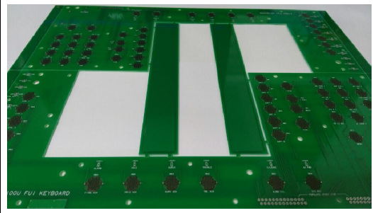
Best Practices for Thermal Management in PCB Electronic Circuit Design
Thermal management is a critical aspect of PCB (Printed Circuit Board) electronic circuit design, as it directly impacts the performance, reliability, and longevity of electronic devices. With the increasing miniaturization and power density of modern electronics, effective heat dissipation has become more challenging yet essential. Poor thermal management can lead to component failure, reduced efficiency, and even safety hazards. This article explores the best practices for thermal management in PCB design, offering actionable insights to engineers and designers to optimize their layouts for better heat dissipation and overall performance.
Component Placement and Layout Optimization
One of the most fundamental aspects of thermal management in PCB design is the strategic placement of components. Heat-generating components, such as power regulators, microprocessors, and high-current drivers, should be spaced apart to prevent localized overheating. Grouping these components too closely can create hotspots, which may degrade performance and shorten the lifespan of the PCB.
Additionally, the layout should facilitate natural airflow. Placing high-heat components near the edges of the board or close to vents can help dissipate heat more effectively. Designers should also consider the orientation of components to maximize exposure to cooling mechanisms, such as fans or heat sinks. Proper component placement not only improves thermal performance but also enhances the overall reliability of the circuit.
Thermal Vias and Copper Pour Techniques
Thermal vias are a powerful tool for dissipating heat in PCBs. These small, plated holes transfer heat from one layer of the board to another, effectively spreading it across the PCB. By placing thermal vias beneath high-heat components, designers can conduct heat away from sensitive areas and toward cooler regions or external heat sinks.
Copper pour techniques further enhance thermal management. Large areas of exposed copper, either on the surface or inner layers, act as heat spreaders. By connecting these copper pours to ground or power planes, designers can create a low-resistance path for heat to travel. The thickness of the copper layers also plays a role; thicker copper can handle more heat, making it ideal for high-power applications.
Heat Sinks and Thermal Interface Materials
Heat sinks are a common solution for managing heat in PCBs, especially for components like CPUs and power transistors. These metal structures absorb and dissipate heat into the surrounding environment. When selecting a heat sink, designers must consider factors such as material (aluminum or copper), size, and fin density to match the thermal requirements of the component.
Thermal interface materials (TIMs), such as thermal pads or pastes, are used to improve the contact between the component and the heat sink. These materials fill microscopic gaps, ensuring efficient heat transfer. Choosing the right TIM is crucial, as poor-quality materials can create thermal resistance, negating the benefits of the heat sink.
PCB Material Selection
The choice of PCB substrate material significantly impacts thermal performance. Standard FR4 is a common choice but has limited thermal conductivity. For high-power applications, materials like metal-core PCBs (MCPCBs) or ceramics offer better heat dissipation. These materials have higher thermal conductivity, allowing them to handle greater thermal loads without compromising performance.
Designers should also consider the dielectric properties of the substrate. Materials with low thermal resistance can help distribute heat more evenly across the board. In some cases, hybrid designs combining different materials may be necessary to balance thermal and electrical performance.
Simulation and Testing
Thermal simulation software is an invaluable tool for predicting heat distribution in PCB designs. By modeling the thermal behavior of the board, designers can identify potential hotspots and optimize their layouts before manufacturing. Tools like computational fluid dynamics (CFD) and finite element analysis (FEA) provide detailed insights into how heat will flow through the PCB.
Physical testing is equally important. Prototypes should undergo thermal imaging and stress testing to validate the design. Real-world conditions, such as varying ambient temperatures and load cycles, can reveal issues that simulations might miss. Iterative testing and refinement ensure the final design meets thermal performance requirements.
By implementing these best practices, designers can create PCBs that efficiently manage heat, ensuring reliable operation and extended lifespan for electronic devices. Thermal management is not just a technical challenge but a cornerstone of successful PCB design.

Essential Tools and Software for Professional PCB Circuit Design
Printed Circuit Board (PCB) design is a critical aspect of modern electronics, enabling the creation of compact, efficient, and reliable electronic devices. Whether you're a hobbyist or a professional, having the right tools and software can make the difference between a successful project and a frustrating experience. This article explores the essential tools and software for professional PCB circuit design, providing insights into how these resources can streamline your workflow, enhance accuracy, and bring your ideas to life.
The world of PCB design has evolved significantly over the years, with advanced software and tools replacing traditional manual methods. Today, designers rely on a combination of schematic capture tools, simulation software, and layout programs to create intricate PCB designs. Understanding these tools and their functionalities is key to mastering PCB design and staying competitive in the fast-paced electronics industry.
Schematic Capture Software
Schematic capture is the first step in PCB design, where the electrical connections and components are laid out in a diagrammatic form. Tools like Altium Designer, KiCad, and OrCAD provide intuitive interfaces for creating schematics, ensuring that all components are correctly connected before moving to the physical layout.
These software solutions often come with extensive libraries of components, allowing designers to drag and drop symbols onto the canvas. Advanced features like real-time error checking and design rule verification help identify potential issues early in the process, saving time and reducing costly mistakes. Additionally, many schematic tools support collaboration, enabling teams to work on the same project simultaneously.
PCB Layout Tools
Once the schematic is complete, the next step is translating it into a physical PCB layout. Software such as Eagle, Altium Designer, and DipTrace offers powerful tools for placing components and routing traces on the board. These programs provide automated routing options, but skilled designers often prefer manual routing for optimal performance.
Modern PCB layout tools also include 3D visualization, allowing designers to see how the final board will look and fit within the enclosure. This feature is invaluable for avoiding mechanical conflicts and ensuring a perfect fit. Furthermore, these tools support multi-layer designs, enabling the creation of complex boards with high component density.
Simulation and Analysis Software
Before manufacturing, it's crucial to simulate the PCB's performance to identify potential issues like signal integrity problems or thermal hotspots. Tools like SPICE (Simulation Program with Integrated Circuit Emphasis) and Ansys SIwave are widely used for circuit simulation and signal integrity analysis.
These simulations can predict how the PCB will behave under various conditions, such as high-frequency signals or extreme temperatures. By running these tests virtually, designers can make necessary adjustments without the need for physical prototypes, reducing both time and costs. Advanced analysis tools also provide insights into electromagnetic compatibility (EMC) and power distribution, ensuring compliance with industry standards.
Manufacturing and Output Tools
After finalizing the design, the next step is preparing the files for manufacturing. Software like Gerber viewers and CAM (Computer-Aided Manufacturing) tools ensure that the design is correctly translated into a format that PCB manufacturers can use. Programs like GerbView and CAM350 help verify that the output files are free of errors and meet the manufacturer's specifications.
These tools also generate essential documentation, such as bill of materials (BOM) and assembly drawings, which are critical for the production process. By automating these tasks, designers can focus on refining their designs rather than dealing with tedious paperwork.
Collaboration and Version Control
In a professional setting, PCB design is often a collaborative effort involving multiple team members. Tools like Git and SVN (Subversion) are commonly used for version control, allowing designers to track changes, revert to previous versions, and merge contributions from different team members.
Cloud-based platforms like Altium 365 and Upverter further enhance collaboration by providing real-time access to design files from anywhere in the world. These platforms often include commenting and review features, making it easier to communicate and iterate on designs efficiently.
Conclusion
Professional PCB circuit design requires a combination of specialized tools and software to ensure accuracy, efficiency, and reliability. From schematic capture and layout to simulation and manufacturing, each step in the process benefits from dedicated solutions that streamline workflows and reduce errors. By leveraging these essential tools, designers can bring their innovative ideas to life and stay ahead in the competitive field of electronics.

Optimizing Power Efficiency in Electronic Circuit Design for PCBs
In the rapidly evolving world of electronics, optimizing power efficiency in printed circuit board (PCB) design has become a critical focus for engineers and designers. As devices grow smaller and more complex, the demand for energy-efficient solutions has skyrocketed. Whether it's for consumer electronics, industrial applications, or IoT devices, reducing power consumption not only extends battery life but also minimizes heat generation and improves overall system reliability. This article delves into the key strategies and techniques for enhancing power efficiency in PCB design, offering valuable insights for professionals aiming to create next-generation electronic systems.
Component Selection and Placement
Choosing the right components is the first step toward optimizing power efficiency in PCB design. Low-power microcontrollers, voltage regulators, and energy-efficient ICs can significantly reduce overall power consumption. For instance, selecting a microcontroller with sleep modes or dynamic voltage scaling can help conserve energy during idle periods. Additionally, using components with lower leakage currents ensures minimal power loss when the device is inactive.
Placement of components on the PCB also plays a crucial role in power efficiency. Properly positioning high-power components away from sensitive analog circuits can reduce interference and improve performance. Grouping related components together minimizes trace lengths, which in turn reduces resistive losses and improves signal integrity. Careful consideration of thermal management during placement can further enhance efficiency by preventing overheating and ensuring stable operation.
Power Distribution Network Design
A well-designed power distribution network (PDN) is essential for maintaining power efficiency in PCBs. The PDN must deliver stable voltage levels to all components while minimizing losses. This begins with selecting appropriate power and ground planes, which provide low-impedance paths for current flow. Using multiple vias for power and ground connections reduces resistance and improves current distribution.
Decoupling capacitors are another critical element of the PDN. Placing them close to power pins of ICs helps suppress noise and stabilize voltage levels. Choosing capacitors with the right capacitance and equivalent series resistance (ESR) ensures optimal performance. Additionally, employing techniques like split power planes or localized voltage regulation can further enhance efficiency by reducing voltage drops and improving power delivery.
Trace Routing and Signal Integrity
Efficient trace routing is vital for minimizing power losses and maintaining signal integrity. Wider traces should be used for high-current paths to reduce resistive losses, while controlled impedance routing is essential for high-speed signals. Avoiding sharp angles and using curved traces can prevent reflections and signal degradation, which indirectly contributes to power efficiency.
Signal integrity is closely tied to power efficiency. Poor signal integrity can lead to retransmissions or increased processing overhead, which consumes additional power. Techniques such as proper termination, impedance matching, and minimizing crosstalk help maintain clean signals and reduce unnecessary power consumption. Additionally, using differential signaling for high-speed interfaces can improve noise immunity and reduce EMI, further enhancing efficiency.
Low-Power Design Techniques
Implementing low-power design techniques is a cornerstone of optimizing power efficiency in PCBs. Dynamic power management, such as clock gating and power gating, allows unused circuit blocks to be turned off when not in use. This approach is particularly effective in battery-powered devices, where every milliwatt counts.
Another technique involves optimizing the operating voltage of components. Running components at the lowest feasible voltage reduces dynamic power consumption, which is proportional to the square of the voltage. Additionally, using energy-efficient communication protocols, such as I2C or SPI, instead of power-hungry alternatives, can further reduce power usage. Combining these techniques with firmware optimizations, such as efficient coding practices and sleep modes, can yield significant power savings.
Thermal Management
Effective thermal management is crucial for maintaining power efficiency in PCBs. Excessive heat can increase resistance in traces and components, leading to higher power losses. Proper heat dissipation techniques, such as using thermal vias, heat sinks, or copper pours, help maintain optimal operating temperatures.
Thermal analysis during the design phase can identify hotspots and guide component placement and routing decisions. For high-power applications, active cooling solutions like fans or liquid cooling may be necessary. By keeping temperatures in check, designers can ensure that components operate within their specified efficiency ranges, ultimately reducing power consumption and improving reliability.
In conclusion, optimizing power efficiency in PCB design requires a holistic approach that encompasses component selection, power distribution, trace routing, low-power techniques, and thermal management. By addressing these aspects, engineers can create energy-efficient electronic systems that meet the demands of modern applications while extending battery life and reducing environmental impact.

Innovative Approaches to Multilayer Rigid Flex Half Hole Technology
Enhanced Design and Routing Strategies
Traditional full-hole vias, while reliable, consume significant space within multilayer rigid-flex PCBs. Half-hole vias, penetrating only halfway through a specific layer, drastically reduce the required space, allowing for denser component placement and more intricate routing. This increased design flexibility is particularly beneficial in applications demanding high component density and complex signal routing, such as wearable electronics, aerospace systems, and advanced medical devices. Sophisticated CAD software and design rules are critical in exploiting the full potential of half-hole technology, ensuring signal integrity and avoiding potential manufacturing challenges. Careful consideration of layer stacking, via placement, and impedance matching are essential for optimizing performance.
Moreover, innovative routing algorithms are being developed to specifically leverage the advantages offered by half-hole technology. These algorithms optimize the placement and connectivity of half-hole vias within the PCB layout, leading to more efficient signal routing and reduced overall board size. The integration of these algorithms into automated design tools streamlines the design process, allowing engineers to quickly and efficiently incorporate half-hole vias into complex PCB designs without compromising signal integrity or manufacturability.
Advanced Laser Drilling Techniques
The precision drilling of half-hole vias demands advanced manufacturing techniques. Laser drilling has emerged as a leading solution, offering superior accuracy and control compared to traditional mechanical drilling methods. Laser ablation allows for highly precise control of the via's depth and diameter, crucial for maintaining consistent impedance and avoiding short circuits in high-density applications. Furthermore, the non-contact nature of laser drilling minimizes damage to surrounding circuitry and substrate materials, enhancing the overall yield and reliability of the finished PCB.
Recent innovations in laser drilling technology include advancements in pulsed laser systems and adaptive control algorithms. Pulsed laser systems offer finer control over energy delivery, allowing for the creation of extremely precise half-holes with smooth, well-defined walls. Adaptive control algorithms monitor the drilling process in real-time, making adjustments to laser parameters to ensure consistent via quality, regardless of variations in material properties or environmental conditions. This enhances the repeatability and reliability of the process, crucial for high-volume manufacturing.
Improved Material Selection and Processing
The successful implementation of half-hole technology also depends on the careful selection of materials and processing techniques. The base materials used in multilayer rigid-flex PCBs must possess excellent mechanical properties, thermal stability, and electrical conductivity to support the demanding environments in which these boards often operate. Furthermore, the choice of plating materials and processes is crucial for ensuring reliable electrical connections within the half-holes.
The development of new dielectric materials with improved thermal conductivity and reduced dielectric constant is actively pursued. These materials can enhance signal transmission speed and reduce signal loss, especially critical in high-frequency applications. Advanced plating techniques, such as electroless plating and immersion plating, are being refined to ensure uniform and reliable metallization of the half-holes, enhancing their conductivity and preventing corrosion.
Challenges and Future Directions
Despite the significant advantages, challenges remain in the widespread adoption of half-hole technology. One key challenge is the need for highly precise manufacturing processes to ensure consistent via quality and prevent defects. Furthermore, the development of robust inspection techniques is essential for verifying the integrity of half-holes after manufacturing. Automated optical inspection (AOI) and other advanced inspection methods are continually improving to address this need.
Future research will focus on further miniaturization of half-holes, allowing for even greater component density. The exploration of new materials and manufacturing processes, along with the development of intelligent design tools, will play a crucial role in overcoming the remaining challenges and unlocking the full potential of multilayer rigid-flex half-hole technology for future generations of advanced electronic devices.
REPORT

