-
 Agriculture
-
 Health-Care
-
 Environment
-
 Construction-Real-Estate
-
 Tools-Hardware
-
 Home-Garden
-
 Furniture
-
 Luggage-Bags-Cases
-
 Medical-devices-Supplies
-
 Gifts-Crafts
-
 Sports-Entertainment
-
 Food-Beverage
-
 Vehicles-Transportation
-
 Power-Transmission
-
 Material-Handling
-
 Renewable-Energy
-
 Safety
-
 Testing-Instrument-Equipment
-
 Construction-Building-Machinery
-
 Pet-Supplies
-
 Personal-Care-Household-Cleaning
-
 Vehicle-Accessories-Electronics-Tools
-
 School-Office-Supplies
-
 Packaging-Printing
-
 Mother-Kids-Toys
-
 Business-Services
-
 Commercial-Equipment-Machinery
-
 Apparel-Accessories
-
 Security
-
 Shoes-Accessories
-
 Vehicle-Parts-Accessories
-
 Jewelry-Eyewear-Watches-Accessories
-
 Lights-Lighting
-
 Fabric-Textile-Raw-Material
-
 Fabrication-Services
-
 Industrial-Machinery
-
 Consumer-Electronics
-
 Electrical-Equipment-Supplies
-
 Electronic-Components-Accessories-Telecommunications
-
 Home-Appliances
-
 Beauty
-
 Chemicals
-
 Rubber-Plastics
-
 Metals-Alloys
- Masonry Materials
- Curtain Walls & Accessories
- Earthwork Products
- Fireproofing Materials
- Heat Insulation Materials
- Plastic Building Materials
- Building Boards
- Soundproofing Materials
- Timber
- Waterproofing Materials
- Balustrades & Handrails
- Bathroom & Kitchen
- Flooring & Accessories
- Tiles & Accessories
- Door, Window & Accessories
- Fireplaces & Stoves
- Floor Heating Systems & Parts
- Stairs & Stair Parts
- Ceilings
- Elevators & Escalators
- Stone
- Countertops, Vanity Tops & Table Tops
- Mosaics
- Metal Building Materials
- Multifunctional Materials
- Ladders & Scaffoldings
- Mouldings
- Corner Guards
- Decorative Films
- Formwork
- Building & Industrial Glass
- Other Construction & Real Estate
- Wallpapers/Wall panels
- HVAC System & Parts
- Outdoor Facilities
- Prefabricated Buildings
- Festive & Party Supplies
- Bathroom Products
- Household Sundries
- Rain Gear
- Garden Supplies
- Household Cleaning Tools & Accessories
- Lighters & Smoking Accessories
- Home Storage & Organization
- Household Scales
- Smart Home Improvement
- Home Textiles
- Kitchenware
- Drinkware & Accessories
- Dinnerware, Coffee & Wine
- Home Decor
- Golf
- Fitness & Body Building
- Amusement Park Facilities
- Billiards, Board Game,Coin Operated Games
- Musical Instruments
- Outdoor Affordable Luxury Sports
- Camping & Hiking
- Fishing
- Sports Safety&Rehabilitation
- Ball Sports Equipments
- Water Sports
- Winter Sports
- Luxury Travel Equipments
- Sports Shoes, Bags & Accessories
- Cycling
- Other Sports & Entertainment Products
- Artificial Grass&Sports Flooring&Sports Court Equipment
- Scooters
- Food Ingredients
- Honey & Honey Products
- Snacks
- Nuts & Kernels
- Seafood
- Plant & Animal Oil
- Beverages
- Fruit & Vegetable Products
- Frog & Escargot
- Bean Products
- Egg Products
- Dairy Products
- Seasonings & Condiments
- Canned Food
- Instant Food
- Baked Goods
- Other Food & Beverage
- Meat & Poultry
- Confectionery
- Grain Products
- Feminie Care
- Hair Care & Styling
- Body Care
- Hands & Feet Care
- Hygiene Products
- Men's Grooming
- Laundry Cleaning Supplies
- Travel Size & Gift Sets
- Room Deodorizers
- Other Personal Care Products
- Pest Control Products
- Special Household Cleaning
- Floor Cleaning
- Kitchen & Bathroom Cleaning
- Oral Care
- Bath Supplies
- Yellow Pages
- Correction Supplies
- Office Binding Supplies
- Office Cutting Supplies
- Board Erasers
- Office Adhesives & Tapes
- Education Supplies
- Pencil Cases & Bags
- Notebooks & Writing Pads
- File Folder Accessories
- Calendars
- Writing Accessories
- Commercial Office Supplies
- Pencil Sharpeners
- Pens
- Letter Pad/Paper
- Paper Envelopes
- Desk Organizers
- Pencils
- Markers & Highlighters
- Filing Products
- Art Supplies
- Easels
- Badge Holder & Accessories
- Office Paper
- Printer Supplies
- Book Covers
- Other Office & School Supplies
- Stationery Set
- Boards
- Clipboards
- Stamps
- Drafting Supplies
- Stencils
- Electronic Dictionary
- Books
- Map
- Magazines
- Calculators
- Baby & Toddler Toys
- Educational Toys
- Classic Toys
- Dress Up & Pretend Play
- Toy Vehicle
- Stuffed Animals & Plush Toys
- Outdoor Toys & Structures
- Balloons & Accessories
- Baby Food
- Children's Clothing
- Baby Supplies & Products
- Maternity Clothes
- Kids Shoes
- Baby Care
- Novelty & Gag Toys
- Dolls & Accessories
- Puzzle & Games
- Blocks & Model Building Toys
- Toddler Clothing
- Baby Clothing
- Kids' Luggage & Bags
- Arts, Crafts & DIY Toys
- Action & Toy Figures
- Baby Appliances
- Hobbies & Models
- Remote Control Toys
- Promotional Toys
- Pregnancy & Maternity
- Hygiene Products
- Kid's Textile&Bedding
- Novelty & Special Use
- Toy Weapons
- Baby Gifts
- Baby Storage & Organization
- Auto Drive Systems
- ATV/UTV Parts & Accessories
- Marine Parts & Accessories
- Other Auto Parts
- Trailer Parts & Accessories
- Auto Transmission Systems
- Train Parts & Accessories
- Universal Parts
- Railway Parts & Accessories
- Auto Brake Systems
- Aviation Parts & Accessories
- Truck Parts & Accessories
- Auto Suspension Systems
- Auto Lighting Systems
- New Energy Vehicle Parts & Accessories
- Auto Steering Systems
- Wheels, Tires & Accessories
- Bus Parts & Accessories
- Auto Performance Parts
- Cooling System
- Go-Kart & Kart Racer Parts & Accessories
- Air Conditioning Systems
- Heavy Duty Vehicle Parts & Accessories
- Auto Electrical Systems
- Auto Body Systems
- Auto Engine Systems
- Container Parts & Accessories
- Motorcycle Parts & Accessories
- Refrigeration & Heat Exchange Equipment
- Machine Tool Equipment
- Food & Beverage Machinery
- Agricultural Machinery & Equipment
- Apparel & Textile Machinery
- Chemical Machinery
- Packaging Machines
- Paper Production Machinery
- Plastic & Rubber Processing Machinery
- Industrial Robots
- Electronic Products Machinery
- Metal & Metallurgy Machinery
- Woodworking Machinery
- Home Product Manufacturing Machinery
- Machinery Accessories
- Environmental Machinery
- Machinery Service
- Electrical Equipment Manufacturing Machinery
- Industrial Compressors & Parts
- Tobacco & Cigarette Machinery
- Production Line
- Used Industrial Machinery
- Electronics Production Machinery
- Other Machinery & Industrial Equipment
- Camera, Photo & Accessories
- Portable Audio, Video & Accessories
- Television, Home Audio, Video & Accessories
- Video Games & Accessories
- Mobile Phone & Accessories
- Electronic Publications
- Earphone & Headphone & Accessories
- Speakers & Accessories
- Smart Electronics
- TV Receivers & Accessories
- Mobile Phone & Computer Repair Parts
- Chargers, Batteries & Power Supplies
- Used Electronics
- VR, AR, MR Hardware & Software
- Projectors & Presentation Equipments
- Other Consumer Electronics
- Cables & Commonly Used Accessories
- Computer Hardware & Software
- Displays, Signage and Optoelectronics
- Discrete Semiconductors
- Wireless & IoT Module and Products
- Telecommunications
- Connectors, Terminals & Accessories
- Development Boards, Electronic Modules and Kits
- Circuit Protection
- Sensors
- Isolators
- Audio Components and Products
- Integrated Circuits
- Power Supplies
- Relays
- RF, Microwave and RFID
- Electronic Accessories & Supplies
- Passive Components
- PCB & PCBA
- Air Quality Appliances
- Home Appliance Parts
- Heating & Cooling Appliances
- Small Kitchen Appliances
- Laundry Appliances
- Water Heaters
- Water Treatment Appliances
- Refrigerators & Freezers
- Personal Care & Beauty Appliances
- Major Kitchen Appliances
- Cleaning Appliances
- Second-hand Appliances
- Smart Home Appliances
- Other Home Appliances
- Energy Chemicals
- Inorganic Chemicals
- Basic Organic Chemicals
- Agrochemicals
- Admixture & Additives
- Catalysts & Chemical Auxiliary Agents
- Pigments & Dyestuff
- Coating & Paint
- Daily Chemicals
- Polymer
- Organic Intermediate
- Adhesives & Sealants
- Chemical Waste
- Biological Chemical Products
- Surface Treatment Chemicals
- Painting & Coating
- Chemical Reagents
- Flavor & Fragrance
- Non-Explosive Demolition Agents
- Other Chemicals
- Custom Chemical Services
PCB & PCBA
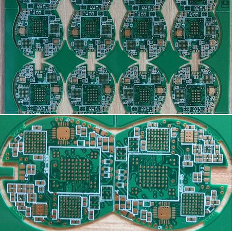
Streamlining The Electronics Layout Process From Schematic To Manufacturing
In the fast-paced world of electronics development, the journey from a conceptual schematic to a tangible, manufacturable printed circuit board (PCB) is often fraught with complexity, potential errors, and time-consuming iterations. Streamlining the electronics layout process from schematic to manufacturing is not merely an operational goal; it is a critical competitive necessity. This integrated approach seeks to bridge the traditional gaps between design, verification, and production, creating a seamless, efficient, and error-resistant workflow. By adopting a holistic strategy that leverages advanced tools, standardized practices, and collaborative principles, companies can dramatically reduce time-to-market, enhance product reliability, and control costs. This article delves into the multifaceted aspects of this streamlining process, exploring how modern methodologies are transforming a traditionally segmented sequence into a cohesive and agile engineering discipline.
The Foundation: Integrated Design Tools and Unified Data Management
The cornerstone of a streamlined process is the adoption of integrated electronic design automation (EDA) software suites. Historically, schematic capture and PCB layout were handled by separate, often poorly communicating tools, leading to manual netlist transfers and synchronization errors. Modern platforms integrate schematic entry, component library management, simulation, PCB layout, and design rule checking into a single environment with a unified database. This integration ensures that any change made in the schematic is automatically reflected in the layout, and vice versa, maintaining consistency and eliminating a major source of human error.
Furthermore, effective data management extends beyond the design tool itself. It involves creating a centralized, cloud-accessible component library with validated footprints, 3D models, and supply chain information. When every engineer uses the same "single source of truth" for components, it prevents mismatches between the schematic symbol and the physical PCB footprint—a common cause of manufacturing re-spins. This unified approach to data management forms the digital backbone that supports all subsequent streamlining efforts, from simulation to fabrication file generation.
Enforcing Intent: Design Rule Checking and Constraint Management
Streamlining requires moving from reactive error detection to proactive design guidance. This is achieved through sophisticated design rule checking (DRC) and electrical rule checking (ERC) engines that are deeply integrated into the layout process. However, the true power lies in constraint management. Engineers can define electrical, physical, and manufacturing constraints upfront—such as high-speed signal timing requirements, impedance control, minimum clearances, and drill sizes—and the layout tool will actively enforce these rules in real-time.
For instance, when routing a high-speed differential pair, the tool can automatically ensure the traces are length-matched, maintain a specific gap, and follow the same layer stackup, all while the designer works. This prevents the tedious and error-prone process of manually measuring and adjusting traces after the fact. By encoding design intent and manufacturing capabilities directly into the tool as constraints, the layout process becomes a guided activity that inherently produces a more manufacturable and higher-performance board on the first attempt.
Bridging the Gap: Collaboration and Design for Manufacturing
A streamlined process actively dismantles the silos between design and production teams. Early and continuous collaboration with PCB fabricators and assembly houses is paramount. This is embodied in the practice of Design for Manufacturing (DFM) and Design for Assembly (DFA). Modern EDA tools can run DFM/DFA checks based on the specific capabilities and preferences of a chosen manufacturer, flagging potential issues like slivers of copper, acid traps, or component placements that hinder automated soldering.
This collaborative mindset extends to using shared review platforms. Instead of exchanging static Gerber files for final approval, teams can share interactive, browser-based visualizations of the PCB where both electrical and mechanical engineers can add comments directly onto the design. This real-time collaboration catches interdisciplinary issues—such as a heatsink interfering with a connector—much earlier in the cycle, avoiding costly late-stage changes. The goal is to make the manufacturer a partner in the design process, not just a recipient of final files.
The Final Handoff: Automated Output Generation and Documentation
The culmination of the streamlined process is a flawless, automated handoff to manufacturing. Inconsistent or incomplete output file generation has historically been a major bottleneck and risk. Modern workflows automate the creation of the entire "manufacturing package." With a single command, the system can generate all necessary files: error-free Gerbers in the correct format, NC drill files, pick-and-place data, bill of materials (BOM), assembly drawings, and test point reports.
This automation is powered by templates and scripts configured to the exact requirements of the fabrication and assembly partners. The BOM can be directly linked to the component library, ensuring part numbers and manufacturer data are accurate and up-to-date. By automating this final, critical step, the process eliminates manual errors in file generation, ensures all stakeholders receive consistent information, and allows the design team to release the product with confidence, knowing that the digital model will translate perfectly into a physical product.

Key Principles Of EMI Reduction Through Careful Electronics Layout Design
In the intricate world of modern electronics, where devices operate at ever-increasing speeds and densities, a silent and invisible challenge persistently threatens performance and regulatory compliance: Electromagnetic Interference (EMI). EMI refers to the disruptive electromagnetic energy emitted from an electronic device that can interfere with the operation of other nearby devices or the device itself. As systems become more compact and functionalities more integrated, the potential for EMI grows exponentially, making its mitigation not merely an afterthought but a fundamental design imperative. While components selection and shielding are crucial, the first and most impactful line of defense lies in the careful, strategic design of the printed circuit board (PCB) layout itself. A well-architected layout can prevent noise generation and coupling at the source, often rendering costly corrective measures like additional shielding unnecessary. This article delves into the key principles of EMI reduction through meticulous electronics layout design, exploring foundational strategies that empower engineers to create robust, reliable, and compliant products from the ground up. By mastering these layout techniques, designers can tame electromagnetic emissions, ensuring their creations function flawlessly in our increasingly connected electromagnetic environment.
Strategic Component Placement and Partitioning
The battle against EMI begins with the strategic placement of components on the PCB. This initial step sets the stage for all subsequent routing and is critical for containing noise. The fundamental rule is to physically separate circuits based on their function and speed. The board should be partitioned into distinct areas: a clean, quiet zone for analog and sensitive circuits (like sensors or RF receivers), a controlled zone for digital processing, and a separate, well-contained zone for high-power or noisy circuits (such as switching regulators, motor drivers, or clock generators).
This partitioning prevents noise from high-speed digital or power sections from capacitively or inductively coupling into sensitive analog traces. Furthermore, components should be placed to minimize the length of critical high-speed traces. Clock generators, oscillators, and drivers should be positioned as close as possible to the devices they serve. By reducing the physical length of these potential antennas, the loop area for radiating electromagnetic energy is significantly minimized, directly reducing emitted interference.
Meticulous Power Distribution Network (PDN) Design
A robust and quiet Power Distribution Network is the cornerstone of a low-EMI design. The primary goal is to provide a stable, low-impedance power source to all ICs across a wide frequency range. A common failure is to treat power traces as simple connections, neglecting their behavior as transmission lines at high frequencies. The use of dedicated power and ground planes in a multilayer board is highly recommended. These planes create a natural distributed capacitance, offering a very low-impedance return path for high-frequency currents.
Decoupling capacitors are vital components of the PDN and must be placed with precision. Large bulk capacitors handle lower frequency demands, while smaller, low-inductance ceramic capacitors (e.g., 0.1µF, 0.01µF) must be placed as close as possible to the power pins of each IC. This proximity is non-negotiable; it minimizes the parasitic inductance of the connection, allowing the capacitor to effectively "short" high-frequency noise on the power rail to ground locally before it can propagate across the board. A multi-value decoupling strategy often works best to address a broad spectrum of noise frequencies.
Controlled Impedance Routing and Signal Integrity
For any high-speed signal—typically where the trace length approaches 1/10th of the signal's wavelength—controlled impedance routing becomes essential. Uncontrolled impedance leads to signal reflections, which manifest as ringing, overshoot, and increased EMI. Traces must be designed as transmission lines with a specific characteristic impedance (e.g., 50Ω, 75Ω) matched to the source and load. This is achieved by carefully calculating and controlling the trace width and its distance to an adjacent reference plane (ground or power).
Critical signals, especially clocks and high-speed data lines, should be routed on layers adjacent to a solid reference plane. This confines the electromagnetic fields between the trace and the plane, reducing both radiation and susceptibility. Furthermore, these traces must be kept short, straight, and avoid sharp 90-degree corners, which can cause impedance discontinuities. Using 45-degree angles or curved traces is preferable. Differential pair routing (for USB, Ethernet, etc.) must maintain consistent spacing (coupling) between the pair and equal length to preserve common-mode noise rejection.
Comprehensive Grounding Strategy
Perhaps no other topic in EMI control is as critical and misunderstood as grounding. A poor ground system is the single largest contributor to EMI problems. The key principle is to minimize ground impedance and avoid ground loops. For mixed-signal boards, the recommended approach is often a single, contiguous ground plane. While intuitively one might think to split analog and digital grounds, this can create more problems than it solves by forcing return currents to take long, inductive paths that increase radiation.
Instead, a unified ground plane provides the lowest impedance return path. Separation is achieved by partitioning the components on the board and carefully routing signals so that high-speed digital return currents do not flow under sensitive analog sections. For systems with very high-noise isolated sections (like a relay driver), a single-point "star" ground connection to the main ground plane may be used. The grounding scheme for cables and shields must also be considered; shield connections should be bonded to the chassis or ground plane at a single, clean point to prevent noise currents from flowing on the shield.
Shielding, Filtering, and Layout Finishing Touches
While a good layout minimizes the need for additional measures, shielding and filtering act as essential safeguards. Filtering involves placing passive components like ferrite beads, inductors, and capacitors at board interfaces (power entry, I/O connectors) to block conducted EMI from entering or leaving the board. These filter components must be placed right at the connector entry point, with their ground connections tied directly to a clean reference plane to be effective.
Finally, attention to layout details is paramount. Avoid leaving unused copper areas floating, as they can act as antennas; tie them to ground. Provide ample stitching vias when a return current must change reference planes, ensuring a continuous low-impedance path. For very sensitive designs, a grounded "guard ring" or trace around a critical circuit can help shunt away stray fields. By integrating these principles from the initial design phase, engineers create a layout that is inherently quiet, turning EMI reduction from a reactive troubleshooting exercise into a proactive design achievement.

Innovative Techniques For Signal Integrity In Electronics Layout Design
In the rapidly evolving landscape of electronics, where data rates soar and device footprints shrink, maintaining signal integrity (SI) has transitioned from a desirable best practice to a non-negotiable cornerstone of successful product design. Signal integrity refers to the preservation of the quality and timing of electrical signals as they traverse the complex pathways of a printed circuit board (PCB). Degradation, manifesting as noise, distortion, or timing errors, can lead to catastrophic system failures, reduced performance, and costly design re-spins. Traditional layout rules, while foundational, are often insufficient to address the challenges posed by modern high-speed digital interfaces, RF communications, and mixed-signal systems. This reality has catalyzed a paradigm shift towards innovative techniques in electronics layout design. These advanced methodologies leverage sophisticated simulation, novel materials, and intelligent topological strategies to predict, mitigate, and control signal integrity issues from the earliest stages of the design cycle. By exploring these cutting-edge approaches, engineers can unlock new levels of performance and reliability, ensuring that their designs not only function but excel in an increasingly demanding technological environment.
Advanced Modeling and Simulation-Driven Design
The era of designing a layout and hoping for the best is long over. Modern signal integrity assurance is fundamentally rooted in predictive, simulation-driven workflows. Innovative techniques now employ 3D full-wave electromagnetic (EM) field solvers that go beyond simple rule-of-thumb calculations. These powerful tools can accurately model complex structures like via transitions, connectors, and intricate package geometries, extracting precise S-parameters and revealing parasitic effects that 2D simulations might miss.
Furthermore, the integration of these simulations directly into the PCB layout environment represents a significant leap forward. Real-time or "in-design" analysis allows engineers to receive immediate feedback on impedance, crosstalk, and eye diagram margins as they route critical nets. This iterative process prevents integrity violations from becoming entrenched, dramatically reducing debugging time later. Another key innovation is the use of statistical analysis and machine learning algorithms to model process variations and worst-case scenarios, ensuring robustness across manufacturing tolerances and environmental conditions.
Innovative Materials and Stack-up Engineering
The physical foundation of the PCB itself is a critical frontier for signal integrity innovation. Advanced laminate materials with tightly controlled dielectric constants (Dk) and dissipation factors (Df) are now essential for high-frequency applications. Low-loss laminates minimize signal attenuation, while materials with stable Dk across frequency and temperature ensure consistent impedance control.
Stack-up design has evolved into a sophisticated co-engineering effort between electrical and mechanical disciplines. Innovative techniques involve the strategic use of hybrid stack-ups, combining different material types within a single board to optimize cost and performance for various signal classes. The placement of power and ground planes is no longer just about providing DC voltage; it is meticulously planned to create controlled return paths, manage electromagnetic interference (EMI), and form embedded capacitance for power integrity, which is intrinsically linked to signal integrity. Techniques like using ultra-thin dielectrics for closer coupling between signal and reference planes are also employed to enhance performance.
Topological Strategies for High-Speed Routing
At the heart of layout design, the routing of traces has seen profound innovation. For parallel bus architectures like DDR memory, advanced fly-by topology with carefully designed on-die termination (ODT) has become standard to manage signal reflections and maintain clean timing across multiple devices. For serial links, the focus is on minimizing loss and preserving the purity of the signal waveform.
Differential pair routing, critical for high-speed serial interfaces, now employs techniques like phase tuning through serpentine routing with minimum impact on impedance, and length matching that accounts for the different propagation velocities in the fiber weave of the laminate. The management of vias, traditional signal integrity weak points, has been revolutionized by the use of back-drilling (controlled depth drilling) to remove unused via stubs, and the implementation of sophisticated via structures such as via-in-pad and microvias in high-density interconnect (HDI) designs to minimize discontinuities.
Power Integrity as a Foundation for Signal Integrity
A stable and clean power delivery network (PDN) is now universally recognized as a prerequisite for good signal integrity. Innovative techniques here focus on achieving target impedance across a broad frequency range. This involves the strategic placement and selection of decoupling capacitors, moving from simple bulk and ceramic caps to a optimized portfolio that addresses mid-frequency and high-frequency noise.
The design of the power and ground planes themselves is critical. Techniques like the use of dedicated power layers, the creation of split planes with careful attention to preventing return path discontinuities, and the implementation of electromagnetic bandgap (EBG) structures to suppress noise propagation are at the forefront. Co-simulation of the PDN with the signal networks allows designers to see how power supply noise directly modulates high-speed signals, enabling a holistic optimization of the entire system.
Addressing Crosstalk and EMI Proactively
As densities increase, unwanted electromagnetic coupling, or crosstalk, becomes a primary threat. Innovative layout techniques proactively manage this through 3D spacing rules, which consider not just horizontal separation but vertical separation between layers. Guard traces with grounded vias are strategically placed to isolate extremely sensitive nets, such as low-amplitude analog signals or clock lines.
Furthermore, signal integrity innovation is deeply intertwined with EMI control. Techniques like edge-rate control through series termination resistors, the use of shielding cans or localized copper fences for noisy circuits, and the careful management of slotting in reference planes are employed to contain electromagnetic emissions at the source. By treating SI and EMI as two sides of the same coin, these integrated techniques ensure the design meets both functional performance and regulatory compliance requirements.
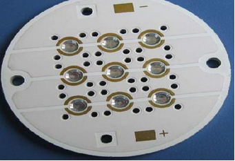
Reliable Light Dimming Technology That Ensures Consistent Illumination And Long Term Durability
In the ever-evolving landscape of lighting solutions, the quest for control, comfort, and efficiency has led to significant advancements in dimming technology. Beyond the simple act of lowering light levels, modern reliable light dimming technology represents a sophisticated integration of electronics, materials science, and user-centric design. Its core promise—ensuring consistent illumination and long-term durability—addresses fundamental pain points in both residential and commercial settings. Flickering lights, inconsistent brightness, premature failure of bulbs or dimmer switches, and compatibility issues have long plagued traditional systems. Today's reliable dimming technologies are engineered to eliminate these frustrations, offering seamless performance that enhances ambiance, saves energy, and stands the test of time. This article delves into the mechanisms and benefits that make such technology indispensable for contemporary lighting design.
The Engineering Behind Flicker-Free and Consistent Dimming
Achieving truly consistent illumination during dimming is a complex challenge that goes beyond merely reducing voltage. Older technologies like leading-edge phase-cut dimmers often caused visible flicker, especially with low-load LED bulbs, and produced an uneven, "steppy" dimming curve. Reliable modern systems employ advanced electronic drivers and microcontrollers that utilize techniques such as pulse-width modulation (PWM) at high frequencies or constant current reduction (CCR). These methods allow for precise, granular control of the light output, enabling a smooth, continuous dimming range from 100% down to 1% or even 0.1% without any perceptible flicker to the human eye.
This consistency is crucial for visual comfort and task performance. In environments like home theaters, restaurants, or offices, the ability to set and maintain a specific light level without fluctuations creates the intended atmosphere and prevents eye strain. The technology ensures that the color temperature and quality of light remain stable across the dimming range, a feature particularly important for high-CRI (Color Rendering Index) lighting where accurate color perception is key. This engineering precision transforms dimming from a crude function into a refined tool for environmental control.
Ensuring Long-Term Durability and Component Integrity
Durability is a cornerstone of reliable dimming technology, extending the lifespan of both the dimmer itself and the connected light fixtures. Inferior dimmers can cause excessive electrical stress on LED drivers, leading to premature burnout and a shortened operational life. Advanced dimmers are built with robust components—such as high-quality semiconductors, thermal management systems, and protective circuits—that handle electrical loads efficiently and dissipate heat effectively.
Furthermore, these systems incorporate comprehensive protection features. These include safeguards against inrush currents (sudden surges when turning on), over-voltage, over-temperature, and short-circuit conditions. By mitigating these stressors, the technology protects the sensitive electronics within LED bulbs or fixtures. This not only ensures the dimmer's own longevity, often rated for tens of thousands of cycles, but also maximizes the lifespan of the often more expensive lighting elements, providing significant long-term value and reducing maintenance costs and electronic waste.
Advanced Compatibility and Smart Integration
One of the historical challenges with dimming has been compatibility, especially with the diverse universe of LED products. A reliable dimming system is designed for broad compatibility, often adhering to or exceeding industry standards like UL, CE, and specific protocols for LED dimming. Many modern dimmers feature auto-adaptive technology or adjustable settings (like minimum load levels) that allow them to automatically calibrate for optimal performance with a wide array of LED, incandescent, and halogen bulbs.
This compatibility extends seamlessly into the realm of smart homes and building automation. Reliable dimming technology forms the backbone of intelligent lighting systems, integrating with protocols like DALI, 0-10V, Zigbee, Z-Wave, or Wi-Fi. This allows for centralized control, scheduling, scene setting, and integration with sensors for occupancy or daylight harvesting. The durability and consistency of the core dimming function ensure that these smart features operate reliably over years, making the system a future-proof investment that supports energy management strategies and enhanced user convenience.
Contributions to Energy Efficiency and User Experience
The benefits of reliable dimming extend directly into energy conservation and superior user experience. By providing precise control over light levels, these systems enable users to use only the amount of light needed, reducing energy consumption significantly compared to fixtures operating at full brightness continuously. This is not merely theoretical; in commercial buildings, automated dimming tied to daylight sensors can yield substantial savings on electricity bills.
From a user perspective, the technology delivers unparalleled comfort and control. The smooth, silent operation without flicker or buzzing noise eliminates distraction. The intuitive interfaces—whether a traditional slider, a touch panel, or a smartphone app—make it easy to create customized lighting scenes for different activities, from focused work to relaxed entertaining. The assurance of durability means this enhanced experience is not temporary; it is a permanent upgrade to the living or working environment, fostering well-being and satisfaction through superior, dependable light quality.
REPORT

