-
 Agriculture
-
 Health-Care
-
 Environment
-
 Construction-Real-Estate
-
 Tools-Hardware
-
 Home-Garden
-
 Furniture
-
 Luggage-Bags-Cases
-
 Medical-devices-Supplies
-
 Gifts-Crafts
-
 Sports-Entertainment
-
 Food-Beverage
-
 Vehicles-Transportation
-
 Power-Transmission
-
 Material-Handling
-
 Renewable-Energy
-
 Safety
-
 Testing-Instrument-Equipment
-
 Construction-Building-Machinery
-
 Pet-Supplies
-
 Personal-Care-Household-Cleaning
-
 Vehicle-Accessories-Electronics-Tools
-
 School-Office-Supplies
-
 Packaging-Printing
-
 Mother-Kids-Toys
-
 Business-Services
-
 Commercial-Equipment-Machinery
-
 Apparel-Accessories
-
 Security
-
 Shoes-Accessories
-
 Vehicle-Parts-Accessories
-
 Jewelry-Eyewear-Watches-Accessories
-
 Lights-Lighting
-
 Fabric-Textile-Raw-Material
-
 Fabrication-Services
-
 Industrial-Machinery
-
 Consumer-Electronics
-
 Electrical-Equipment-Supplies
-
 Electronic-Components-Accessories-Telecommunications
-
 Home-Appliances
-
 Beauty
-
 Chemicals
-
 Rubber-Plastics
-
 Metals-Alloys
- Masonry Materials
- Curtain Walls & Accessories
- Earthwork Products
- Fireproofing Materials
- Heat Insulation Materials
- Plastic Building Materials
- Building Boards
- Soundproofing Materials
- Timber
- Waterproofing Materials
- Balustrades & Handrails
- Bathroom & Kitchen
- Flooring & Accessories
- Tiles & Accessories
- Door, Window & Accessories
- Fireplaces & Stoves
- Floor Heating Systems & Parts
- Stairs & Stair Parts
- Ceilings
- Elevators & Escalators
- Stone
- Countertops, Vanity Tops & Table Tops
- Mosaics
- Metal Building Materials
- Multifunctional Materials
- Ladders & Scaffoldings
- Mouldings
- Corner Guards
- Decorative Films
- Formwork
- Building & Industrial Glass
- Other Construction & Real Estate
- Wallpapers/Wall panels
- HVAC System & Parts
- Outdoor Facilities
- Prefabricated Buildings
- Festive & Party Supplies
- Bathroom Products
- Household Sundries
- Rain Gear
- Garden Supplies
- Household Cleaning Tools & Accessories
- Lighters & Smoking Accessories
- Home Storage & Organization
- Household Scales
- Smart Home Improvement
- Home Textiles
- Kitchenware
- Drinkware & Accessories
- Dinnerware, Coffee & Wine
- Home Decor
- Golf
- Fitness & Body Building
- Amusement Park Facilities
- Billiards, Board Game,Coin Operated Games
- Musical Instruments
- Outdoor Affordable Luxury Sports
- Camping & Hiking
- Fishing
- Sports Safety&Rehabilitation
- Ball Sports Equipments
- Water Sports
- Winter Sports
- Luxury Travel Equipments
- Sports Shoes, Bags & Accessories
- Cycling
- Other Sports & Entertainment Products
- Artificial Grass&Sports Flooring&Sports Court Equipment
- Scooters
- Food Ingredients
- Honey & Honey Products
- Snacks
- Nuts & Kernels
- Seafood
- Plant & Animal Oil
- Beverages
- Fruit & Vegetable Products
- Frog & Escargot
- Bean Products
- Egg Products
- Dairy Products
- Seasonings & Condiments
- Canned Food
- Instant Food
- Baked Goods
- Other Food & Beverage
- Meat & Poultry
- Confectionery
- Grain Products
- Feminie Care
- Hair Care & Styling
- Body Care
- Hands & Feet Care
- Hygiene Products
- Men's Grooming
- Laundry Cleaning Supplies
- Travel Size & Gift Sets
- Room Deodorizers
- Other Personal Care Products
- Pest Control Products
- Special Household Cleaning
- Floor Cleaning
- Kitchen & Bathroom Cleaning
- Oral Care
- Bath Supplies
- Yellow Pages
- Correction Supplies
- Office Binding Supplies
- Office Cutting Supplies
- Board Erasers
- Office Adhesives & Tapes
- Education Supplies
- Pencil Cases & Bags
- Notebooks & Writing Pads
- File Folder Accessories
- Calendars
- Writing Accessories
- Commercial Office Supplies
- Pencil Sharpeners
- Pens
- Letter Pad/Paper
- Paper Envelopes
- Desk Organizers
- Pencils
- Markers & Highlighters
- Filing Products
- Art Supplies
- Easels
- Badge Holder & Accessories
- Office Paper
- Printer Supplies
- Book Covers
- Other Office & School Supplies
- Stationery Set
- Boards
- Clipboards
- Stamps
- Drafting Supplies
- Stencils
- Electronic Dictionary
- Books
- Map
- Magazines
- Calculators
- Baby & Toddler Toys
- Educational Toys
- Classic Toys
- Dress Up & Pretend Play
- Toy Vehicle
- Stuffed Animals & Plush Toys
- Outdoor Toys & Structures
- Balloons & Accessories
- Baby Food
- Children's Clothing
- Baby Supplies & Products
- Maternity Clothes
- Kids Shoes
- Baby Care
- Novelty & Gag Toys
- Dolls & Accessories
- Puzzle & Games
- Blocks & Model Building Toys
- Toddler Clothing
- Baby Clothing
- Kids' Luggage & Bags
- Arts, Crafts & DIY Toys
- Action & Toy Figures
- Baby Appliances
- Hobbies & Models
- Remote Control Toys
- Promotional Toys
- Pregnancy & Maternity
- Hygiene Products
- Kid's Textile&Bedding
- Novelty & Special Use
- Toy Weapons
- Baby Gifts
- Baby Storage & Organization
- Auto Drive Systems
- ATV/UTV Parts & Accessories
- Marine Parts & Accessories
- Other Auto Parts
- Trailer Parts & Accessories
- Auto Transmission Systems
- Train Parts & Accessories
- Universal Parts
- Railway Parts & Accessories
- Auto Brake Systems
- Aviation Parts & Accessories
- Truck Parts & Accessories
- Auto Suspension Systems
- Auto Lighting Systems
- New Energy Vehicle Parts & Accessories
- Auto Steering Systems
- Wheels, Tires & Accessories
- Bus Parts & Accessories
- Auto Performance Parts
- Cooling System
- Go-Kart & Kart Racer Parts & Accessories
- Air Conditioning Systems
- Heavy Duty Vehicle Parts & Accessories
- Auto Electrical Systems
- Auto Body Systems
- Auto Engine Systems
- Container Parts & Accessories
- Motorcycle Parts & Accessories
- Refrigeration & Heat Exchange Equipment
- Machine Tool Equipment
- Food & Beverage Machinery
- Agricultural Machinery & Equipment
- Apparel & Textile Machinery
- Chemical Machinery
- Packaging Machines
- Paper Production Machinery
- Plastic & Rubber Processing Machinery
- Industrial Robots
- Electronic Products Machinery
- Metal & Metallurgy Machinery
- Woodworking Machinery
- Home Product Manufacturing Machinery
- Machinery Accessories
- Environmental Machinery
- Machinery Service
- Electrical Equipment Manufacturing Machinery
- Industrial Compressors & Parts
- Tobacco & Cigarette Machinery
- Production Line
- Used Industrial Machinery
- Electronics Production Machinery
- Other Machinery & Industrial Equipment
- Camera, Photo & Accessories
- Portable Audio, Video & Accessories
- Television, Home Audio, Video & Accessories
- Video Games & Accessories
- Mobile Phone & Accessories
- Electronic Publications
- Earphone & Headphone & Accessories
- Speakers & Accessories
- Smart Electronics
- TV Receivers & Accessories
- Mobile Phone & Computer Repair Parts
- Chargers, Batteries & Power Supplies
- Used Electronics
- VR, AR, MR Hardware & Software
- Projectors & Presentation Equipments
- Other Consumer Electronics
- Cables & Commonly Used Accessories
- Computer Hardware & Software
- Displays, Signage and Optoelectronics
- Discrete Semiconductors
- Wireless & IoT Module and Products
- Telecommunications
- Connectors, Terminals & Accessories
- Development Boards, Electronic Modules and Kits
- Circuit Protection
- Sensors
- Isolators
- Audio Components and Products
- Integrated Circuits
- Power Supplies
- Relays
- RF, Microwave and RFID
- Electronic Accessories & Supplies
- Passive Components
- PCB & PCBA
- Air Quality Appliances
- Home Appliance Parts
- Heating & Cooling Appliances
- Small Kitchen Appliances
- Laundry Appliances
- Water Heaters
- Water Treatment Appliances
- Refrigerators & Freezers
- Personal Care & Beauty Appliances
- Major Kitchen Appliances
- Cleaning Appliances
- Second-hand Appliances
- Smart Home Appliances
- Other Home Appliances
- Energy Chemicals
- Inorganic Chemicals
- Basic Organic Chemicals
- Agrochemicals
- Admixture & Additives
- Catalysts & Chemical Auxiliary Agents
- Pigments & Dyestuff
- Coating & Paint
- Daily Chemicals
- Polymer
- Organic Intermediate
- Adhesives & Sealants
- Chemical Waste
- Biological Chemical Products
- Surface Treatment Chemicals
- Painting & Coating
- Chemical Reagents
- Flavor & Fragrance
- Non-Explosive Demolition Agents
- Other Chemicals
- Custom Chemical Services
Electronic Accessories & Supplies

In the high-stakes world of broadcast television and film production, every detail matters. The difference between a good broadcast and a great one often lies in the quality of lighting, which directly impacts how audiences perceive color, texture, and emotion on screen. For decades, achieving the perfect, consistent, and true-to-life illumination required for professional studios was a complex challenge, often reliant on traditional lighting systems that were energy-intensive and generated significant heat. Today, a technological revolution is illuminating broadcast studios: High-Performance LED Lighting Printed Circuit Boards (PCBs). These are not ordinary LED boards; they are precision-engineered systems designed specifically to meet the exacting demands of broadcast environments, with the core mission of achieving perfect color rendering. This article delves into the sophisticated engineering behind these specialized PCBs, exploring how they are transforming studio lighting by delivering unparalleled color accuracy, reliability, and control, thereby becoming the unseen heroes behind the flawless visuals we see on our screens.
The Paramount Importance of Color Rendering Index (CRI) and Spectral Accuracy
At the heart of broadcast lighting is the need for perfect color fidelity. The Color Rendering Index (CRI) is a quantitative measure of a light source's ability to reveal the true colors of objects compared to a natural reference light. For critical applications like broadcasting, where skin tones, product colors, and set details must be reproduced without distortion, a high CRI is non-negotiable. High-performance LED PCBs for studios are engineered to achieve CRI values of 95 and above, with many targeting CRI 97+ or even perfect scores for specific spectral metrics like R9 (saturated red), which is crucial for accurate flesh tones.
This achievement goes beyond simply using high-CRI LEDs. The PCB itself plays a critical role. Engineers meticulously design the circuit layout and select substrate materials to ensure stable electrical delivery to each LED chip. Any variance in voltage or current can cause slight shifts in color temperature and output, degrading CRI performance. Furthermore, these PCBs often integrate multiple LED chips emitting different wavelengths (not just standard white LEDs). By carefully mixing light from precise red, green, blue, and sometimes amber or mint green emitters, the PCB can create a broad, continuous spectrum that closely mimics natural daylight, filling in spectral gaps that cause poor color rendering in inferior lights.
Advanced Thermal Management for Consistency and Longevity
LED performance is intrinsically linked to temperature. As LEDs heat up, their light output can decrease, and more critically, their chromaticity can shift—a phenomenon known as color drift. In a broadcast setting, a light that changes color temperature during a long recording is unacceptable. Therefore, the thermal design of the lighting PCB is arguably as important as its optical design.
High-performance studio LED PCBs are built on metal-core PCBs (MCPCBs), typically using aluminum or copper substrates. These materials excel at drawing heat away from the LED junctions rapidly. The PCB layout is optimized with large thermal pads and traces to act as heat spreaders. This foundational cooling is often coupled with an external heatsink designed as part of the overall luminaire. The result is a system that maintains the LED chips at a stable, low operating temperature. This thermal stability ensures consistent color output over time, prevents dimming, and significantly extends the operational lifespan of the fixture, which is vital for the 24/7 operational schedules of many broadcast facilities.
Precision Dimming and Flicker-Free Performance
Broadcast lighting requires dynamic control. Scenes may call for subtle dimming or rapid adjustments without any visible artifacts. Traditional dimming methods like Pulse Width Modulation (PWM) can introduce flicker, which may not be visible to the naked eye but can cause devastating strobe effects or banding when captured by high-speed cameras or under certain shutter speeds. High-performance LED PCBs address this with sophisticated driver circuitry integrated directly onto or meticulously paired with the board.
These drivers utilize high-frequency PWM or, more preferably, constant current reduction (CCR) or analog dimming techniques. By operating at frequencies far beyond the capture capability of any camera (often tens or hundreds of kHz) and ensuring smooth current regulation, the PCB delivers truly flicker-free light. This allows cinematographers and lighting directors to dim lights to very low levels without any risk of introducing noise or distortion into the video signal, enabling creative flexibility and ensuring technical perfection under any shooting condition.
Robustness, Reliability, and Control Integration
A broadcast studio is a demanding environment where equipment is frequently adjusted, moved, and must perform reliably for thousands of hours. The LED PCB is engineered for this rugged reality. This involves using high-quality, industrial-grade components, conformal coatings to protect against dust and moisture, and robust mechanical mounting points. The electrical design includes protections against voltage spikes, short circuits, and electrostatic discharge (ESD), which are common in studio settings with lots of cabling and equipment.
Moreover, these intelligent PCBs are designed for seamless integration into modern digital control networks. They often feature built-in interfaces for industry-standard protocols like DMX512, RDM, or DALI. This allows each lighting fixture, guided by its internal PCB, to be individually addressed and controlled from a central console. Lighting directors can create, save, and recall complex lighting scenes with precise control over intensity and color temperature for each fixture, enabling the consistent and repeatable lighting setups that professional production demands. The high-performance PCB is the enabling engine that makes this smart, reliable, and integrated lighting ecosystem possible, ultimately empowering creators to achieve visual storytelling with perfect color rendering at its core.

State Of The Art TV Station Illumination Circuitry For Crystal Clear High Definition Broadcasting
In the dynamic world of modern broadcasting, achieving crystal clear high-definition (HD) and ultra-high-definition (UHD) imagery is paramount. While cameras, lenses, and production software often steal the spotlight, the unsung hero enabling this visual fidelity is state-of-the-art television station illumination circuitry. This sophisticated technology goes far beyond simply turning lights on; it represents a complex ecosystem of intelligent control, precision engineering, and spectral management designed to create the perfect lighting environment for flawless on-air presentation. The transition from standard definition to HD, 4K, and now 8K has exponentially increased the demand for lighting that is not only bright and consistent but also meticulously controllable to reveal detail without harsh shadows or color distortion. This article delves into the core technological pillars that make contemporary broadcast illumination a critical component in the quest for unparalleled picture quality.
Intelligent Digital Control and Dimming Systems
The heart of modern broadcast lighting lies in its digital control infrastructure. Gone are the days of simple analog rheostats. Today's systems utilize advanced protocols like DMX512, RDM (Remote Device Management), and increasingly, Ethernet-based systems like Art-Net or sACN. These protocols allow for the centralized, pixel-precise control of thousands of individual fixtures from a single console.
This intelligence enables lighting directors to create, save, and recall complex lighting scenes instantaneously. For a news broadcast, this might mean a seamless transition from the anchor desk to a weather green screen with perfectly balanced chroma key lighting. Furthermore, modern digital dimming is exceptionally smooth and flicker-free, a non-negotiable requirement for high-frame-rate and slow-motion HD cameras. The circuitry ensures that dimming curves are linear and consistent across all fixtures, eliminating color temperature shifts that can occur with traditional phase-cut dimming, thereby maintaining color integrity under all lighting intensities.
Advanced LED Engine Technology and Spectral Precision
The widespread adoption of Light Emitting Diode (LED) technology has revolutionized broadcast lighting. State-of-the-art circuitry is built specifically to harness the potential of advanced LED engines. These fixtures utilize high-CRI (Color Rendering Index) and TLCI (Television Lighting Consistency Index) optimized LEDs that emit a full and accurate spectrum of light, ensuring that on-screen colors—from skin tones to graphic elements—are reproduced faithfully.
The supporting circuitry manages power delivery, thermal output, and spectral mixing with extreme precision. In RGBW (Red, Green, Blue, White) or full-spectrum tunable fixtures, microprocessors control the output of individual LED color channels. This allows a single fixture to produce any color temperature from warm 2800K to daylight 5600K, or even saturated colors, all with stable, flicker-free performance. This spectral precision is crucial for matching multiple light sources in a studio and for ensuring consistency across different camera sensors, which is fundamental for multi-camera HD productions.
Power Management and Electrical Stability
Broadcast environments are electrically sensitive ecosystems. State-of-the-art illumination circuitry incorporates robust power conditioning and management to ensure absolute stability. Voltage fluctuations or electrical noise can introduce visible flicker in cameras or cause inconsistent light output, which is catastrophic for live HD broadcasting.
Modern power supplies within lighting fixtures are designed to be highly efficient and generate minimal electromagnetic interference (EMI). This is complemented by studio-wide power distribution units that provide clean, regulated power to entire lighting grids. Additionally, with the high density of LED fixtures in modern studios, thermal management is engineered into the circuitry. Efficient heat sinks and active cooling systems, controlled by thermal sensors, prevent overheating—which can lead to color shift, reduced LED lifespan, and potential failure—ensuring reliable operation during long broadcast days.
Integration with Broadcast Automation and Virtual Sets
The frontier of broadcast lighting lies in its deep integration with other production systems. State-of-the-art circuitry enables lighting to be a dynamic data-driven element rather than a static setup. Through network integration, lighting consoles can receive triggers from broadcast automation systems. This allows lighting scenes to change automatically in sync with camera cuts, graphic roll-ins, or segment transitions, adding a layer of polished dynamism to the broadcast.
This integration is especially critical for virtual and augmented reality studio environments. Here, the physical lighting on the talent and green screen must perfectly match the virtual environment's lighting model to create a believable composite. Advanced circuitry allows lighting parameters (like direction, intensity, and color) to be controlled in real-time based on data from the graphics engine, ensuring that virtual shadows and highlights align perfectly with the real-world subject, which is essential for maintaining the illusion of a cohesive, high-definition scene.
In conclusion, state-of-the-art TV station illumination circuitry forms the technological backbone that makes crystal clear high-definition broadcasting possible. It is a synergistic blend of digital control, spectral science, stable power engineering, and system-wide integration. As broadcast resolutions continue to climb and production techniques become more complex, the role of this intelligent, precise, and reliable lighting technology will only grow more central, ensuring that the picture delivered to viewers remains impeccably clear, vibrant, and true to life.

Innovative Television Station PCB Engineering Ensuring Optimal Illumination And Energy Efficiency
In the dynamic world of broadcast media, the relentless pursuit of superior picture quality and operational sustainability has driven television stations to the forefront of technological innovation. At the heart of this evolution lies a critical, yet often overlooked, component: the Printed Circuit Board (PCB). The engineering of PCBs for modern television stations is no longer just about connecting electronic components; it has transformed into a sophisticated discipline focused on ensuring optimal on-screen illumination and unparalleled energy efficiency. This intricate engineering forms the backbone of everything from high-definition studio cameras and advanced lighting control systems to the powerful transmitters that broadcast signals worldwide. As viewers demand brighter, more vivid images and regulators impose stricter energy consumption standards, the role of innovative PCB design becomes paramount. This article delves into the multifaceted engineering breakthroughs that allow contemporary television stations to deliver stunning visual experiences while championing environmental and economic responsibility through intelligent, energy-conscious design.
The Integration of Advanced LED Driver Circuits and Thermal Management
A cornerstone of achieving optimal illumination in television production is the precise control of modern LED lighting arrays, which have largely replaced traditional incandescent and fluorescent sources. The PCBs designed for these systems incorporate highly specialized LED driver circuits. These are not simple power supplies; they are complex, feedback-driven systems engineered for stability and accuracy. They utilize pulse-width modulation (PWM) techniques at very high frequencies to eliminate flicker—a critical requirement for high-speed camera work—while providing granular dimming control. This allows lighting directors to create the exact ambiance and exposure needed for any scene, from a brightly lit news desk to a dramatically shadowed drama set, all while maintaining perfect color temperature consistency crucial for broadcast colorimetry.
However, driving high-power LEDs generates significant heat, which can degrade performance, shift color output, and drastically shorten component lifespan. Therefore, innovative PCB engineering directly addresses thermal management. This involves the strategic use of metal-core PCBs (MCPCBs), where a base layer of aluminum or copper acts as a heat sink, drawing thermal energy away from the LED chips and their drivers. The layout, or topology, of the PCB is meticulously planned to separate heat-generating components and incorporate wide thermal relief pads and vias that channel heat to dedicated heat dissipation layers. This synergy between electrical design and thermal engineering ensures that lighting systems deliver maximum luminous efficacy—more light per watt of electrical input—which is the fundamental link between brilliant illumination and energy savings.
Intelligent Power Distribution and Voltage Regulation Systems
Beyond individual lighting units, the entire power infrastructure of a television station relies on innovatively engineered PCBs to minimize energy waste. Modern broadcast facilities employ distributed power architecture systems, where AC power is converted to a stable DC voltage at a central point and then distributed efficiently throughout the facility. The PCBs within these power distribution units (PDUs) and point-of-load (POL) regulators are designed for peak efficiency. They utilize synchronous rectification, low-loss MOSFETs, and high-frequency switching to reduce energy lost as heat during conversion and regulation. This ensures that cameras, servers, routers, and lighting grids receive clean, stable power with minimal transmission losses.
Furthermore, intelligent power management is embedded into the PCB design of various studio equipment. Microcontrollers and dedicated power management ICs (PMICs) on these boards monitor power consumption in real-time. They can dynamically scale voltage and clock speeds of processing chips during lower demand periods or put entire subsystems into low-power sleep modes when not in active use—such as between recording takes or during standby periods. This granular control, facilitated by the PCB's embedded intelligence, eliminates the phantom loads and constant full-power operation that characterized older broadcast equipment, leading to substantial reductions in a station's overall carbon footprint and electricity costs.
Signal Integrity and Low-Noise Design for Enhanced Image Processing
Optimal on-screen illumination is not solely about the physical lights; it is equally about how the camera sensor captures and the broadcast chain processes that light. Any electrical noise or signal degradation introduced by PCBs can manifest as visual artifacts, reduced contrast, or color inaccuracies, forcing equipment to work harder (and consume more power) to compensate. Therefore, PCB engineering for broadcast-grade cameras, vision mixers, and encoders prioritizes impeccable signal integrity. This involves employing multi-layer board designs with dedicated ground planes to shield sensitive analog and high-speed digital signals, such as those from a camera's CCD or CMOS sensor.
Careful routing techniques are used to prevent crosstalk between adjacent traces carrying critical video data. The selection of components with low electromagnetic interference (EMI) characteristics and the strategic placement of decoupling capacitors near every integrated circuit are standard practices. By ensuring the purest possible signal path from image capture to transmission, these PCBs enable the use of more efficient video compression algorithms (like HEVC/H.265) that require cleaner source material. A clean signal compresses more efficiently, reducing the bitrate needed for a given quality level, which in turn lowers the power required for processing, storage, and transmission—a direct contribution to system-wide energy efficiency.
Adaptive Control Systems and the Role of the Internet of Things (IoT)
The final layer of innovation lies in connectivity and adaptive control. Modern television station PCBs are increasingly equipped with IoT-enabled microcontrollers and network interfaces, such as Ethernet or wireless modules. This transforms passive equipment into nodes on an intelligent network. Lighting rigs, for instance, can be controlled via IP-based protocols like Art-Net or sACN, where commands travel over data networks instead of dedicated, less efficient DMX cables. The PCBs within each fixture can receive complex commands to adjust intensity and color based on pre-programmed scenes or even real-time sensor data.
This connectivity allows for the implementation of sophisticated, building-wide energy management systems. Sensors monitoring ambient studio light, occupancy, or even the specific camera shot being used can feed data back to a central controller. This system can then automatically dim or brighten lights in unused areas of a set or adjust the entire studio's lighting profile to match the optimal configuration for a specific production, all executed through commands processed by the local PCBs in each device. This level of automation ensures that energy is consumed only where and when it is needed with surgical precision, marrying the goals of perfect creative illumination and minimal energy expenditure through the intelligence embedded in the station's engineered circuitry.
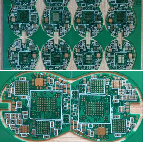
Ceramic Board Advancements Supporting Miniaturization And Power In Microwave RF PCB Designs
The relentless drive toward smaller, more powerful, and higher-frequency electronic systems, particularly in telecommunications, aerospace, defense, and automotive radar, places immense pressure on the foundational materials used in circuit design. Traditional organic substrates like FR-4 often reach their performance limits in demanding Microwave and Radio Frequency (RF) applications, struggling with signal loss, thermal management, and dimensional stability at elevated frequencies. This is where the article "Ceramic Board Advancements Supporting Miniaturization And Power In Microwave RF PCB Designs" enters the spotlight, addressing a critical technological nexus. It explores how cutting-edge developments in ceramic-based circuit boards are not merely incremental improvements but are enabling paradigm shifts in design. By delving into the material science and engineering breakthroughs behind ceramics such as Aluminum Nitride (AlN), Low-Temperature Co-Fired Ceramic (LTCC), and High-Temperature Co-Fired Ceramic (HTCC), the piece illuminates their pivotal role in overcoming the twin challenges of miniaturization and increased power density. For engineers and designers pushing the boundaries of 5G/6G infrastructure, satellite communications, and advanced radar systems, understanding these advancements is key to unlocking the next generation of high-performance, compact RF modules.
Superior Electrical Properties for High-Frequency Performance
The cornerstone of ceramic board utility in RF design lies in their exceptional electrical characteristics. Unlike standard PCB materials, advanced ceramics exhibit a very low dielectric loss tangent (tan δ). This property is paramount at microwave frequencies, as it directly correlates to signal attenuation. Minimal dielectric loss ensures that RF signals propagate through the substrate with far less energy dissipated as heat, preserving signal integrity and enabling higher efficiency in power amplifiers and low-noise receivers.
Furthermore, ceramics offer a range of stable dielectric constants (Dk). This stability, maintained over a wide temperature and frequency range, allows for precise and predictable control of impedance. Designers can create transmission lines, filters, and antennas with consistent performance, which is critical for complex RF systems. The ability to select ceramics with specific Dk values also aids in miniaturization, as a higher Dk allows for physically smaller wavelength structures, directly contributing to the reduction of circuit footprint without sacrificing electrical length or performance.
Unmatched Thermal Management Capabilities
As RF power levels increase and components are packed more densely, managing waste heat becomes a primary design constraint. Ceramic substrates excel in this domain due to their high thermal conductivity. Materials like Aluminum Nitride (AlN) and Beryllium Oxide (BeO) possess thermal conductivity values orders of magnitude greater than conventional FR-4, rivaling even some metals.
This exceptional thermal performance serves a dual purpose. Firstly, it acts as an efficient heat spreader, pulling heat away from active devices like power amplifiers, MMICs (Monolithic Microwave Integrated Circuits), and transistors. This prevents the formation of localized hot spots that can degrade performance and reliability. Secondly, by efficiently transferring heat to a heatsink or chassis, ceramics enable systems to operate at higher continuous power levels or in higher ambient temperatures. This directly supports the trend toward higher power density, allowing more functionality to be integrated into a smaller space without thermal throttling or failure.
Enabling High-Density Integration and Miniaturization
Ceramic technologies, particularly LTCC and HTCC, are instrumental in achieving system-level miniaturization. These processes allow for the creation of multilayer, three-dimensional circuit structures within a single, monolithic ceramic package. Passive components such as resistors, inductors, capacitors, and intricate transmission line structures can be embedded within the ceramic layers during the firing process.
This embedded component technology is a game-changer for miniaturization. It eliminates the need for numerous surface-mounted discrete components, saving valuable board real estate and reducing parasitic inductances and capacitances associated with solder joints and leads. The result is a highly integrated, compact module that offers improved RF performance and enhanced reliability. Additionally, the fine line and spacing resolution achievable with ceramic processes support the design of compact, high-frequency circuits necessary for millimeter-wave applications, making ceramics indispensable for the ongoing miniaturization of RF front-end modules.
Mechanical and Environmental Stability
The robustness of ceramic materials under harsh conditions provides a significant reliability advantage. Ceramic boards exhibit excellent dimensional stability; they have a very low coefficient of thermal expansion (CTE) that can be closely matched to that of semiconductor dies (like GaAs or GaN). This matching minimizes thermomechanical stress at critical solder and wire-bond joints during temperature cycling, greatly enhancing the long-term reliability of the assembly.
Moreover, ceramics are inherently hermetic, impervious to moisture absorption, and resistant to most chemicals and radiation. This makes them ideal for applications in extreme environments, such as space, military, and down-hole drilling equipment, where organic PCBs would quickly fail. This environmental resilience ensures consistent electrical performance over the product's lifetime, regardless of operating conditions, which is a non-negotiable requirement in many high-reliability RF applications.
Material and Process Innovations
The advancements supporting miniaturization and power are driven by continuous innovation in both ceramic materials and fabrication processes. The development of new ceramic composites and formulations aims to optimize the trade-offs between dielectric constant, loss tangent, thermal conductivity, and cost. For instance, advancements in AlN processing have made it more commercially viable for high-power applications.
On the process front, innovations in fine-line printing, laser drilling for micro-vias, and precision patterning enable higher circuit density and more complex multilayer architectures. Additive manufacturing techniques for ceramics are also emerging, promising unprecedented design freedom for creating custom, non-planar RF structures. These material and process innovations collectively push the boundaries of what is possible, allowing ceramic boards to meet the ever-increasing demands for performance, size, and power in next-generation microwave and RF systems.
REPORT


