-
 Agriculture
-
 Health-Care
-
 Environment
-
 Construction-Real-Estate
-
 Tools-Hardware
-
 Home-Garden
-
 Furniture
-
 Luggage-Bags-Cases
-
 Medical-devices-Supplies
-
 Gifts-Crafts
-
 Sports-Entertainment
-
 Food-Beverage
-
 Vehicles-Transportation
-
 Power-Transmission
-
 Material-Handling
-
 Renewable-Energy
-
 Safety
-
 Testing-Instrument-Equipment
-
 Construction-Building-Machinery
-
 Pet-Supplies
-
 Personal-Care-Household-Cleaning
-
 Vehicle-Accessories-Electronics-Tools
-
 School-Office-Supplies
-
 Packaging-Printing
-
 Mother-Kids-Toys
-
 Business-Services
-
 Commercial-Equipment-Machinery
-
 Apparel-Accessories
-
 Security
-
 Shoes-Accessories
-
 Vehicle-Parts-Accessories
-
 Jewelry-Eyewear-Watches-Accessories
-
 Lights-Lighting
-
 Fabric-Textile-Raw-Material
-
 Fabrication-Services
-
 Industrial-Machinery
-
 Consumer-Electronics
-
 Electrical-Equipment-Supplies
-
 Electronic-Components-Accessories-Telecommunications
-
 Home-Appliances
-
 Beauty
-
 Chemicals
-
 Rubber-Plastics
-
 Metals-Alloys
- Masonry Materials
- Curtain Walls & Accessories
- Earthwork Products
- Fireproofing Materials
- Heat Insulation Materials
- Plastic Building Materials
- Building Boards
- Soundproofing Materials
- Timber
- Waterproofing Materials
- Balustrades & Handrails
- Bathroom & Kitchen
- Flooring & Accessories
- Tiles & Accessories
- Door, Window & Accessories
- Fireplaces & Stoves
- Floor Heating Systems & Parts
- Stairs & Stair Parts
- Ceilings
- Elevators & Escalators
- Stone
- Countertops, Vanity Tops & Table Tops
- Mosaics
- Metal Building Materials
- Multifunctional Materials
- Ladders & Scaffoldings
- Mouldings
- Corner Guards
- Decorative Films
- Formwork
- Building & Industrial Glass
- Other Construction & Real Estate
- Wallpapers/Wall panels
- HVAC System & Parts
- Outdoor Facilities
- Prefabricated Buildings
- Festive & Party Supplies
- Bathroom Products
- Household Sundries
- Rain Gear
- Garden Supplies
- Household Cleaning Tools & Accessories
- Lighters & Smoking Accessories
- Home Storage & Organization
- Household Scales
- Smart Home Improvement
- Home Textiles
- Kitchenware
- Drinkware & Accessories
- Dinnerware, Coffee & Wine
- Home Decor
- Golf
- Fitness & Body Building
- Amusement Park Facilities
- Billiards, Board Game,Coin Operated Games
- Musical Instruments
- Outdoor Affordable Luxury Sports
- Camping & Hiking
- Fishing
- Sports Safety&Rehabilitation
- Ball Sports Equipments
- Water Sports
- Winter Sports
- Luxury Travel Equipments
- Sports Shoes, Bags & Accessories
- Cycling
- Other Sports & Entertainment Products
- Artificial Grass&Sports Flooring&Sports Court Equipment
- Scooters
- Food Ingredients
- Honey & Honey Products
- Snacks
- Nuts & Kernels
- Seafood
- Plant & Animal Oil
- Beverages
- Fruit & Vegetable Products
- Frog & Escargot
- Bean Products
- Egg Products
- Dairy Products
- Seasonings & Condiments
- Canned Food
- Instant Food
- Baked Goods
- Other Food & Beverage
- Meat & Poultry
- Confectionery
- Grain Products
- Feminie Care
- Hair Care & Styling
- Body Care
- Hands & Feet Care
- Hygiene Products
- Men's Grooming
- Laundry Cleaning Supplies
- Travel Size & Gift Sets
- Room Deodorizers
- Other Personal Care Products
- Pest Control Products
- Special Household Cleaning
- Floor Cleaning
- Kitchen & Bathroom Cleaning
- Oral Care
- Bath Supplies
- Yellow Pages
- Correction Supplies
- Office Binding Supplies
- Office Cutting Supplies
- Board Erasers
- Office Adhesives & Tapes
- Education Supplies
- Pencil Cases & Bags
- Notebooks & Writing Pads
- File Folder Accessories
- Calendars
- Writing Accessories
- Commercial Office Supplies
- Pencil Sharpeners
- Pens
- Letter Pad/Paper
- Paper Envelopes
- Desk Organizers
- Pencils
- Markers & Highlighters
- Filing Products
- Art Supplies
- Easels
- Badge Holder & Accessories
- Office Paper
- Printer Supplies
- Book Covers
- Other Office & School Supplies
- Stationery Set
- Boards
- Clipboards
- Stamps
- Drafting Supplies
- Stencils
- Electronic Dictionary
- Books
- Map
- Magazines
- Calculators
- Baby & Toddler Toys
- Educational Toys
- Classic Toys
- Dress Up & Pretend Play
- Toy Vehicle
- Stuffed Animals & Plush Toys
- Outdoor Toys & Structures
- Balloons & Accessories
- Baby Food
- Children's Clothing
- Baby Supplies & Products
- Maternity Clothes
- Kids Shoes
- Baby Care
- Novelty & Gag Toys
- Dolls & Accessories
- Puzzle & Games
- Blocks & Model Building Toys
- Toddler Clothing
- Baby Clothing
- Kids' Luggage & Bags
- Arts, Crafts & DIY Toys
- Action & Toy Figures
- Baby Appliances
- Hobbies & Models
- Remote Control Toys
- Promotional Toys
- Pregnancy & Maternity
- Hygiene Products
- Kid's Textile&Bedding
- Novelty & Special Use
- Toy Weapons
- Baby Gifts
- Baby Storage & Organization
- Auto Drive Systems
- ATV/UTV Parts & Accessories
- Marine Parts & Accessories
- Other Auto Parts
- Trailer Parts & Accessories
- Auto Transmission Systems
- Train Parts & Accessories
- Universal Parts
- Railway Parts & Accessories
- Auto Brake Systems
- Aviation Parts & Accessories
- Truck Parts & Accessories
- Auto Suspension Systems
- Auto Lighting Systems
- New Energy Vehicle Parts & Accessories
- Auto Steering Systems
- Wheels, Tires & Accessories
- Bus Parts & Accessories
- Auto Performance Parts
- Cooling System
- Go-Kart & Kart Racer Parts & Accessories
- Air Conditioning Systems
- Heavy Duty Vehicle Parts & Accessories
- Auto Electrical Systems
- Auto Body Systems
- Auto Engine Systems
- Container Parts & Accessories
- Motorcycle Parts & Accessories
- Refrigeration & Heat Exchange Equipment
- Machine Tool Equipment
- Food & Beverage Machinery
- Agricultural Machinery & Equipment
- Apparel & Textile Machinery
- Chemical Machinery
- Packaging Machines
- Paper Production Machinery
- Plastic & Rubber Processing Machinery
- Industrial Robots
- Electronic Products Machinery
- Metal & Metallurgy Machinery
- Woodworking Machinery
- Home Product Manufacturing Machinery
- Machinery Accessories
- Environmental Machinery
- Machinery Service
- Electrical Equipment Manufacturing Machinery
- Industrial Compressors & Parts
- Tobacco & Cigarette Machinery
- Production Line
- Used Industrial Machinery
- Electronics Production Machinery
- Other Machinery & Industrial Equipment
- Camera, Photo & Accessories
- Portable Audio, Video & Accessories
- Television, Home Audio, Video & Accessories
- Video Games & Accessories
- Mobile Phone & Accessories
- Electronic Publications
- Earphone & Headphone & Accessories
- Speakers & Accessories
- Smart Electronics
- TV Receivers & Accessories
- Mobile Phone & Computer Repair Parts
- Chargers, Batteries & Power Supplies
- Used Electronics
- VR, AR, MR Hardware & Software
- Projectors & Presentation Equipments
- Other Consumer Electronics
- Cables & Commonly Used Accessories
- Computer Hardware & Software
- Displays, Signage and Optoelectronics
- Discrete Semiconductors
- Wireless & IoT Module and Products
- Telecommunications
- Connectors, Terminals & Accessories
- Development Boards, Electronic Modules and Kits
- Circuit Protection
- Sensors
- Isolators
- Audio Components and Products
- Integrated Circuits
- Power Supplies
- Relays
- RF, Microwave and RFID
- Electronic Accessories & Supplies
- Passive Components
- PCB & PCBA
- Air Quality Appliances
- Home Appliance Parts
- Heating & Cooling Appliances
- Small Kitchen Appliances
- Laundry Appliances
- Water Heaters
- Water Treatment Appliances
- Refrigerators & Freezers
- Personal Care & Beauty Appliances
- Major Kitchen Appliances
- Cleaning Appliances
- Second-hand Appliances
- Smart Home Appliances
- Other Home Appliances
- Energy Chemicals
- Inorganic Chemicals
- Basic Organic Chemicals
- Agrochemicals
- Admixture & Additives
- Catalysts & Chemical Auxiliary Agents
- Pigments & Dyestuff
- Coating & Paint
- Daily Chemicals
- Polymer
- Organic Intermediate
- Adhesives & Sealants
- Chemical Waste
- Biological Chemical Products
- Surface Treatment Chemicals
- Painting & Coating
- Chemical Reagents
- Flavor & Fragrance
- Non-Explosive Demolition Agents
- Other Chemicals
- Custom Chemical Services
Smart Electronics
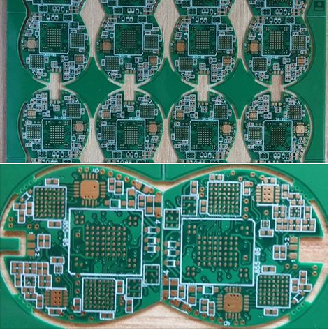
Cutting Edge Solutions via 10 Layers HDI FR4 PCB Technology
In the rapidly evolving world of electronics, the demand for high-performance, compact, and reliable printed circuit boards (PCBs) has never been greater. Cutting Edge Solutions via 10 Layers HDI FR4 PCB Technology represents a significant leap forward in meeting these demands. High-Density Interconnect (HDI) PCBs, combined with the robust FR4 material, offer unparalleled advantages in terms of signal integrity, thermal management, and space efficiency. This technology is particularly crucial for applications in aerospace, medical devices, telecommunications, and consumer electronics, where precision and reliability are paramount.
The 10-layer HDI FR4 PCB is a marvel of modern engineering, enabling designers to pack more functionality into smaller spaces while maintaining high performance. By leveraging advanced manufacturing techniques such as laser drilling and sequential lamination, these PCBs achieve finer lines and spaces, higher connection densities, and improved electrical performance. This article delves into the various aspects of this cutting-edge technology, exploring its benefits, applications, and future potential.
Unmatched Performance and Signal Integrity
One of the standout features of 10-layer HDI FR4 PCBs is their ability to maintain exceptional signal integrity even in the most demanding environments. The multiple layers allow for better distribution of power and ground planes, reducing electromagnetic interference (EMI) and crosstalk between signals. This is particularly important for high-frequency applications, where signal degradation can lead to performance issues.
Furthermore, the use of FR4 material, known for its excellent dielectric properties, ensures stable signal transmission across all layers. The combination of HDI technology and FR4 results in a PCB that can handle complex circuits with minimal signal loss, making it ideal for advanced communication systems and high-speed computing devices.
Space Efficiency and Miniaturization
The 10-layer HDI FR4 PCB excels in space efficiency, a critical factor in today's trend toward miniaturization. With electronic devices becoming smaller and more powerful, the need for compact yet high-performance PCBs has grown exponentially. HDI technology allows for the placement of components on both sides of the board and the use of microvias to connect layers, significantly reducing the overall footprint.
This miniaturization is achieved without compromising functionality. In fact, the dense interconnections enabled by HDI technology often result in improved performance, as shorter trace lengths reduce latency and power consumption. This makes 10-layer HDI FR4 PCBs a preferred choice for smartphones, wearables, and other portable devices where space is at a premium.
Enhanced Thermal Management
Thermal management is a critical consideration in PCB design, especially for high-power applications. The 10-layer HDI FR4 PCB addresses this challenge through its multi-layer structure, which provides better heat dissipation compared to traditional PCBs. The additional layers allow for the incorporation of thermal vias and heat sinks, effectively channeling heat away from sensitive components.
FR4 material itself has good thermal stability, but when combined with HDI technology, the PCB can handle higher power densities without overheating. This makes it suitable for applications such as power supplies, automotive electronics, and industrial control systems, where thermal performance is crucial for reliability and longevity.
Versatility and Broad Applications
The versatility of 10-layer HDI FR4 PCBs is another reason for their widespread adoption. These PCBs can be customized to meet the specific needs of various industries, from aerospace to medical devices. For instance, in aerospace, the lightweight and high-reliability characteristics of HDI FR4 PCBs make them ideal for avionics and satellite systems.
In the medical field, the precision and reliability of these PCBs are essential for life-saving equipment such as MRI machines and pacemakers. The ability to withstand harsh environments and maintain performance under stress ensures that 10-layer HDI FR4 PCBs are a trusted solution across multiple sectors.
Future Prospects and Innovations
As technology continues to advance, the potential for 10-layer HDI FR4 PCBs is boundless. Innovations in materials and manufacturing processes are expected to further enhance their performance, making them even more efficient and cost-effective. The integration of artificial intelligence and IoT devices will likely drive demand for these PCBs, as they offer the perfect balance of size, performance, and reliability.
Moreover, the push toward greener technologies may lead to the development of more sustainable FR4 materials, reducing the environmental impact of PCB production. With ongoing research and development, 10-layer HDI FR4 PCBs are poised to remain at the forefront of electronic design for years to come.

10 Layers HDI FR4 PCB Technology Enhances Circuit Density
In the rapidly evolving world of electronics, the demand for higher circuit density and more compact designs has never been greater. One of the key technologies enabling this advancement is the 10 Layers HDI (High-Density Interconnect) FR4 PCB (Printed Circuit Board) technology. This innovative approach to PCB design allows for more components to be packed into a smaller space, enhancing performance and functionality while reducing the overall size of electronic devices. As industries such as telecommunications, automotive, and consumer electronics push the boundaries of miniaturization, understanding how 10 Layers HDI FR4 PCB technology enhances circuit density becomes crucial.
HDI technology has revolutionized PCB manufacturing by enabling finer lines, smaller vias, and higher connection pad density. FR4, a widely used substrate material, provides excellent electrical insulation and mechanical strength, making it an ideal choice for multilayer PCBs. By combining these two technologies, manufacturers can create highly complex and dense circuits that meet the demands of modern electronics. This article explores the various ways in which 10 Layers HDI FR4 PCB technology enhances circuit density, offering insights into its benefits and applications.
Increased Layer Count for Enhanced Circuit Density
The most obvious advantage of a 10-layer HDI FR4 PCB is the increased number of layers, which directly translates to higher circuit density. With ten layers, designers have more room to route traces and place components, reducing the need for bulky and space-consuming designs. This multilayer approach allows for better signal integrity and reduced electromagnetic interference (EMI), as signals can be routed more efficiently between layers.
Moreover, the additional layers enable the use of dedicated power and ground planes, which further enhances the performance of the PCB. By separating power and ground layers, designers can minimize noise and improve the overall stability of the circuit. This is particularly important in high-speed and high-frequency applications, where signal integrity is paramount.
Advanced Via Technologies for Miniaturization
HDI technology is characterized by its use of advanced via structures, such as microvias, blind vias, and buried vias. These vias are significantly smaller than traditional through-hole vias, allowing for more connections to be made in a smaller area. In a 10-layer HDI FR4 PCB, microvias can be used to connect adjacent layers, reducing the need for long traces and freeing up valuable space for additional components.
Blind and buried vias further enhance circuit density by enabling connections between specific layers without affecting the entire board. This targeted approach to routing allows for more efficient use of space and reduces the overall size of the PCB. Additionally, the use of stacked and staggered microvias can further increase the density of connections, making it possible to design highly complex circuits in a compact form factor.
Improved Material Properties for Higher Performance
FR4 is a popular substrate material for PCBs due to its excellent electrical insulation, mechanical strength, and thermal stability. When used in a 10-layer HDI configuration, FR4 provides a stable foundation for high-density circuits. The material's low dielectric constant and loss tangent ensure minimal signal loss, even at high frequencies, making it suitable for advanced applications such as 5G communications and high-speed data transmission.
Furthermore, FR4's thermal properties help dissipate heat effectively, preventing overheating and ensuring the reliability of the PCB. This is particularly important in high-density designs, where the proximity of components can lead to increased thermal stress. By combining FR4 with HDI technology, manufacturers can create PCBs that are not only dense but also highly reliable and durable.
Enhanced Design Flexibility and Innovation
The combination of 10-layer HDI and FR4 technology offers unparalleled design flexibility, enabling engineers to push the boundaries of innovation. With more layers and advanced via technologies, designers can create highly customized and optimized circuits tailored to specific applications. This flexibility is particularly valuable in industries such as aerospace and medical devices, where space constraints and performance requirements are critical.
Additionally, the ability to integrate passive components, such as resistors and capacitors, directly into the PCB further enhances circuit density. This embedded component technology reduces the need for surface-mounted devices, freeing up space for other components and simplifying the assembly process. As a result, 10-layer HDI FR4 PCBs are at the forefront of modern electronics design, enabling smaller, faster, and more efficient devices.
Conclusion
10 Layers HDI FR4 PCB technology represents a significant leap forward in circuit density and performance. By leveraging advanced via technologies, increased layer counts, and the superior properties of FR4, manufacturers can create highly dense and reliable PCBs that meet the demands of today's electronics industry. As the need for miniaturization and high-performance continues to grow, this technology will play an increasingly important role in shaping the future of electronic design.

Innovative Designs with 10 Layers HDI FR4 PCB Technology
In the rapidly evolving world of electronics, the demand for high-performance, compact, and reliable printed circuit boards (PCBs) has never been greater. Innovative designs with 10 Layers HDI FR4 PCB Technology are at the forefront of this revolution, offering unparalleled capabilities for advanced applications. Whether it's for aerospace, medical devices, or high-speed computing, this technology enables engineers to push the boundaries of what's possible. But what exactly makes 10-layer HDI FR4 PCBs so special? Let's delve into the details.
High-Density Interconnect (HDI) technology, combined with the robustness of FR4 material, provides a perfect balance of performance and durability. The 10-layer configuration allows for complex routing and high signal integrity, making it ideal for modern electronic designs. As we explore the various aspects of this technology, you'll gain a deeper understanding of its benefits and applications.
Unmatched Design Flexibility
One of the standout features of 10-layer HDI FR4 PCBs is their exceptional design flexibility. With multiple layers, engineers can distribute power and ground planes more effectively, reducing noise and improving signal quality. This is particularly important for high-frequency applications where signal integrity is paramount.
Moreover, the use of microvias and blind/buried vias in HDI technology allows for tighter component placement and more efficient use of board space. This means that even the most complex designs can be accommodated without sacrificing performance or reliability. The result is a PCB that not only meets but exceeds the demands of modern electronics.
Enhanced Signal Integrity
Signal integrity is a critical factor in the performance of any electronic device. With 10-layer HDI FR4 PCBs, the multiple layers provide dedicated spaces for signal traces, power planes, and ground planes. This separation minimizes crosstalk and electromagnetic interference (EMI), ensuring clean and reliable signal transmission.
Additionally, the use of advanced materials like FR4, known for its excellent dielectric properties, further enhances signal integrity. The combination of HDI technology and FR4 material results in a PCB that can handle high-speed signals with minimal loss or distortion. This makes it an ideal choice for applications such as telecommunications and data centers.
Superior Thermal Management
Thermal management is another area where 10-layer HDI FR4 PCBs excel. The multiple layers allow for better heat dissipation, which is crucial for high-power applications. By strategically placing thermal vias and heat sinks, engineers can effectively manage the temperature of the PCB, preventing overheating and ensuring long-term reliability.
FR4 material itself has good thermal stability, but when combined with the layered structure of an HDI PCB, the thermal performance is significantly enhanced. This is particularly beneficial for applications like automotive electronics and industrial control systems, where temperature fluctuations are common.
Cost-Effective Solution
While 10-layer HDI FR4 PCBs offer advanced features, they are also a cost-effective solution for many applications. The ability to integrate multiple functions into a single board reduces the need for additional components and assemblies, lowering overall production costs.
Furthermore, the durability and reliability of FR4 material mean that these PCBs have a longer lifespan, reducing the need for frequent replacements. This makes them a smart investment for businesses looking to balance performance and budget.
Wide Range of Applications
The versatility of 10-layer HDI FR4 PCBs makes them suitable for a wide range of applications. From consumer electronics to military and aerospace, these PCBs are used in industries that demand high performance and reliability.
In the medical field, for example, they are used in advanced imaging systems and portable diagnostic devices. In the automotive industry, they power everything from infotainment systems to advanced driver-assistance systems (ADAS). The possibilities are virtually endless, thanks to the innovative design capabilities of this technology.
In conclusion, 10-layer HDI FR4 PCB Technology represents a significant leap forward in electronic design. Its unmatched flexibility, enhanced signal integrity, superior thermal management, cost-effectiveness, and wide range of applications make it a game-changer in the industry. As technology continues to advance, we can expect even more innovative designs to emerge, further solidifying the importance of this remarkable technology.

Seamless 5G Connectivity Via Rigid Flex PCB Smartphone
The advent of 5G technology has revolutionized the way we connect and communicate, demanding faster, more reliable, and efficient hardware solutions. One such innovation is the integration of Rigid Flex PCBs (Printed Circuit Boards) in smartphones, enabling seamless 5G connectivity. This breakthrough not only enhances performance but also paves the way for sleeker, more durable designs. As 5G networks continue to expand globally, the need for advanced circuitry that can handle high-frequency signals without compromising on space or durability has never been greater. This article delves into how Rigid Flex PCBs are transforming smartphones into powerful 5G devices.
The Role of Rigid Flex PCBs in 5G Smartphones
Rigid Flex PCBs combine the best of both rigid and flexible circuit boards, offering unparalleled versatility for modern smartphones. Unlike traditional PCBs, which are either rigid or flexible, Rigid Flex PCBs integrate both types into a single unit. This hybrid design allows for more compact and lightweight smartphones, which is crucial for accommodating the complex antenna systems required for 5G connectivity.
Moreover, Rigid Flex PCBs provide superior signal integrity, a critical factor for 5G networks that operate at higher frequencies. The reduced signal loss and interference ensure that users experience faster download and upload speeds, lower latency, and more stable connections. This makes Rigid Flex PCBs an ideal choice for next-generation smartphones.
Enhanced Durability and Space Efficiency
One of the standout features of Rigid Flex PCBs is their durability. Traditional rigid PCBs are prone to cracking under stress, while flexible PCBs may wear out over time. Rigid Flex PCBs, however, offer the perfect balance, with rigid sections providing structural support and flexible sections allowing for bending and folding. This makes smartphones more resistant to physical damage, such as drops and impacts.
Additionally, the space-saving design of Rigid Flex PCBs allows manufacturers to maximize the internal layout of smartphones. With 5G requiring more components, such as multiple antennas and advanced cooling systems, the compact nature of Rigid Flex PCBs ensures that all these elements fit seamlessly into increasingly slim devices. This efficiency is a game-changer for smartphone design.
Improved Thermal Management
5G technology generates more heat than its predecessors, posing a challenge for smartphone manufacturers. Rigid Flex PCBs address this issue by offering better thermal management compared to traditional PCBs. The materials used in Rigid Flex PCBs dissipate heat more effectively, preventing overheating and ensuring optimal performance.
Furthermore, the flexible sections of the PCB can be strategically placed to avoid heat-sensitive components, reducing the risk of thermal damage. This not only prolongs the lifespan of the smartphone but also enhances user experience by maintaining consistent performance during intensive tasks like gaming or streaming.
Future Prospects and Innovations
The integration of Rigid Flex PCBs in smartphones is just the beginning. As 5G technology evolves, we can expect further advancements in PCB design to meet the growing demands for speed and efficiency. Innovations such as embedded components and advanced materials will likely play a significant role in the next wave of 5G smartphones.
Moreover, the adoption of Rigid Flex PCBs is not limited to smartphones. Other devices, such as wearables and IoT gadgets, can also benefit from this technology, paving the way for a more connected and efficient future. The possibilities are endless, and Rigid Flex PCBs are at the forefront of this technological revolution.
REPORT

